Arizona Semiconductor Ecosystem

America's New Silicon Desert

Arizona has emerged as the global hub for advanced semiconductor manufacturing — with over $200 billion in committed investment from TSMC, Intel, and the broader supply chain, anchoring the United States' most ambitious domestic chip production expansion in history.

$200B+ Committed Investment
40,000+ Jobs Created
5 Leading Fabs
#1 CHIPS Act State
3nm Leading-Edge Node

Semiconductor Facilities Across Arizona

Key fabs, OSATs, design centers, and supply chain companies across the state

Key Facilities & Campuses

Major semiconductor operations anchoring Arizona's manufacturing ecosystem
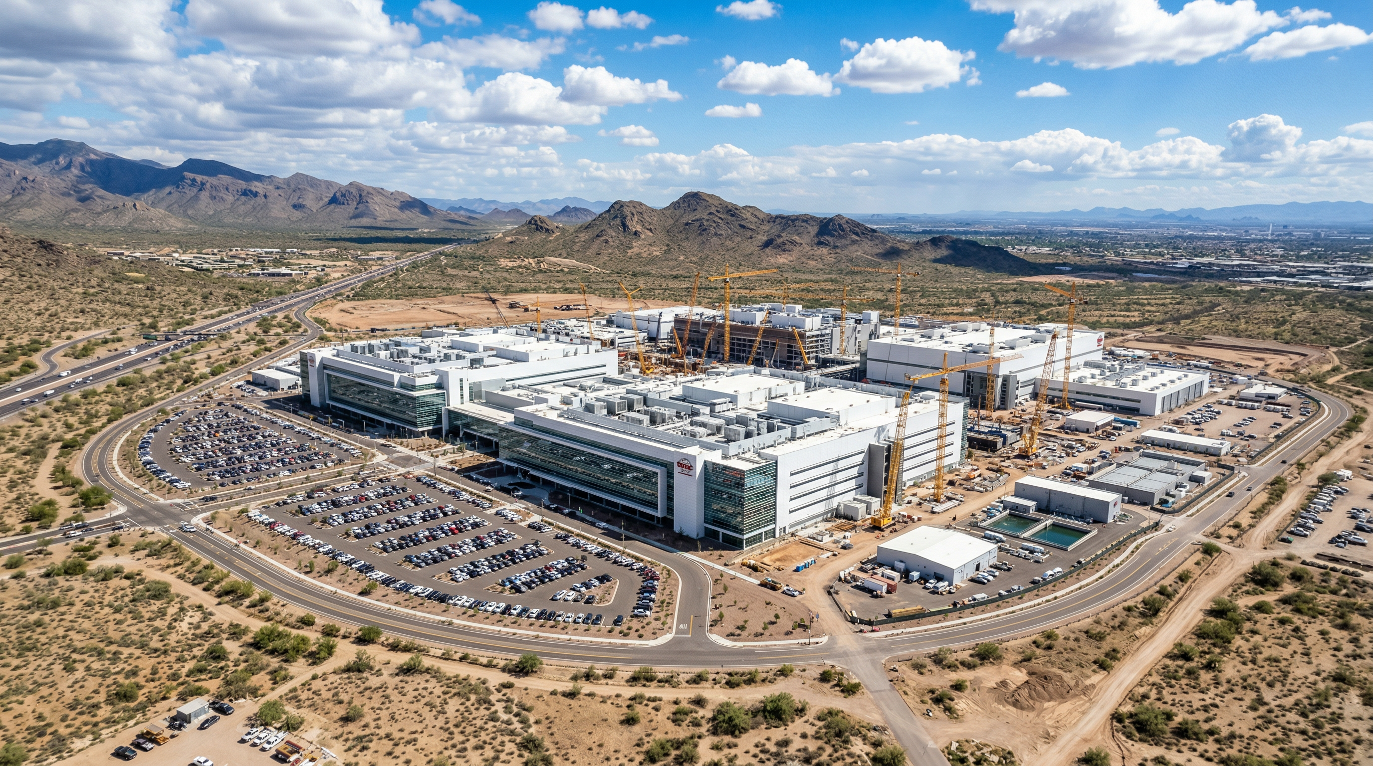
TSMC Fab 21
North Phoenix, AZ — Near 43rd Ave & Loop 303
World's leading foundry. Fab 21 Phase 1 producing 4nm chips; Phase 2 producing 2nm; Phase 3+ planned. $165B total committed investment — the largest foreign direct investment in U.S. history.
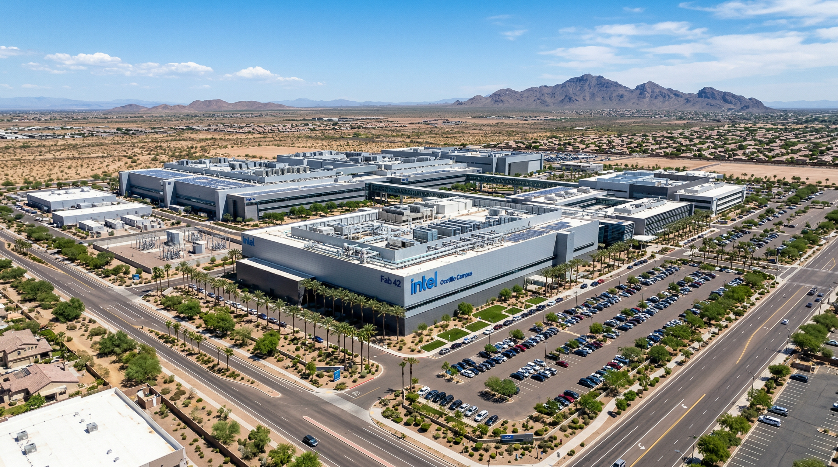
Intel Fab 52 & 62
Chandler, AZ
Intel's Ocotillo campus — two advanced fabs producing Intel 18A and Intel 20A process chips. $20B+ expansion under CHIPS Act funding.
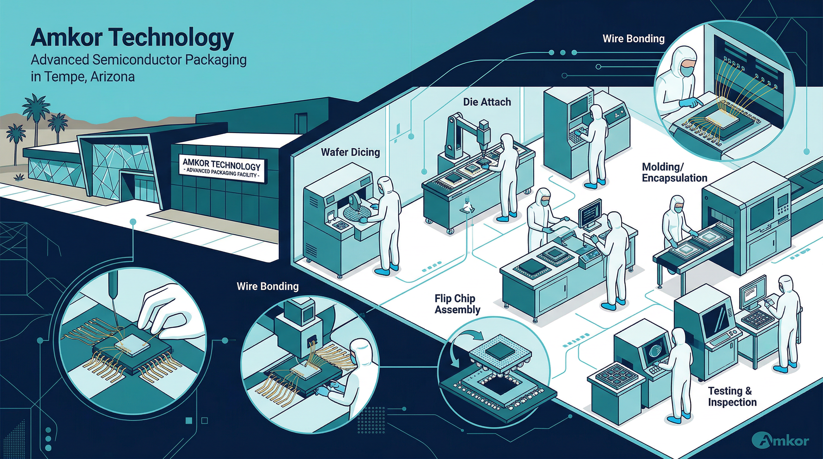
Amkor Technology
Tempe & Peoria, AZ
Global leader in outsourced semiconductor assembly and test (OSAT). Advanced packaging, flip-chip, and wafer-level packaging services for Apple, Qualcomm, and more.
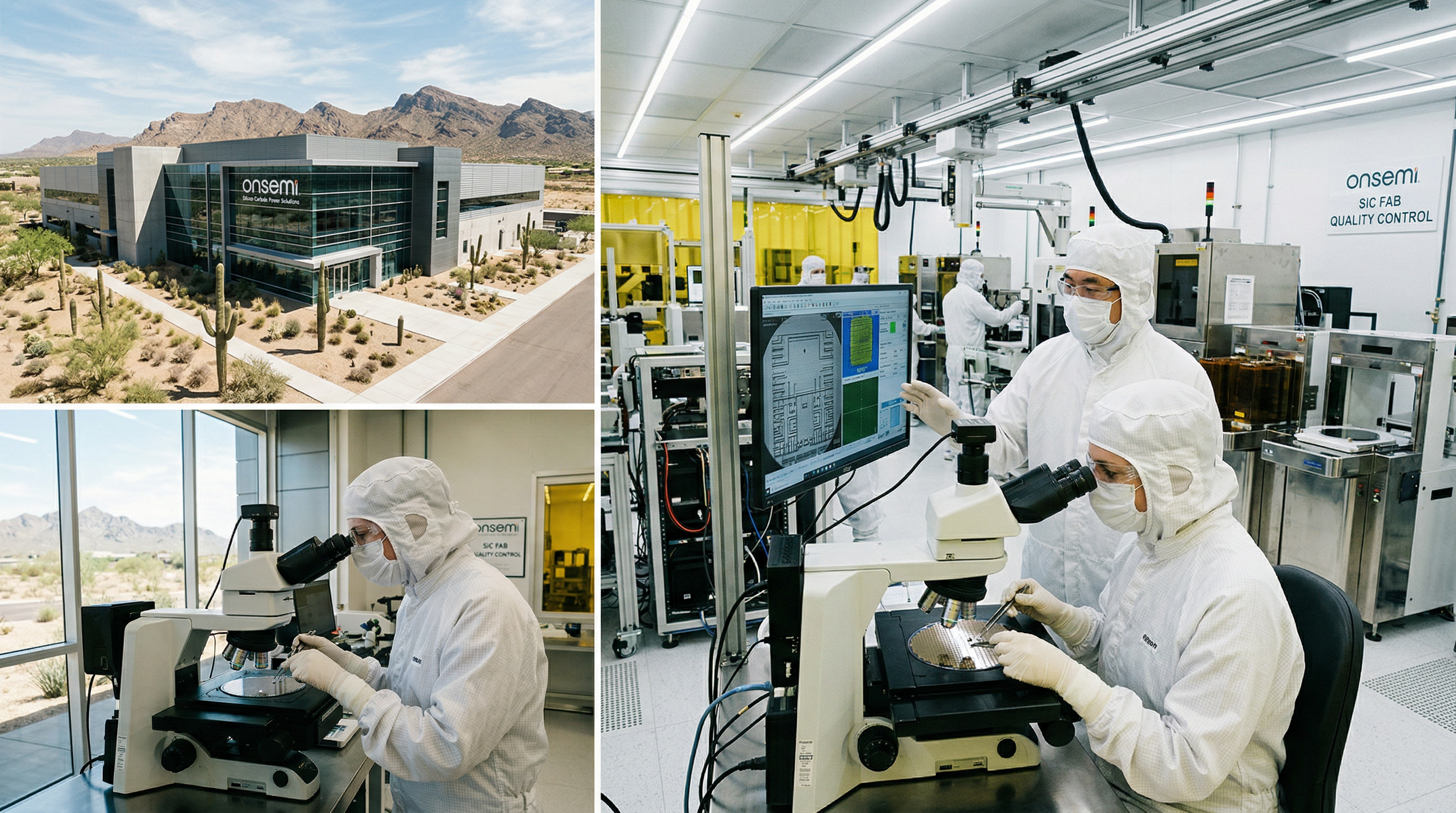
onsemi
Scottsdale & Phoenix, AZ
Headquartered in Scottsdale. Manufactures power semiconductors and image sensors for automotive, EV, and industrial markets. Multiple Arizona fabs.
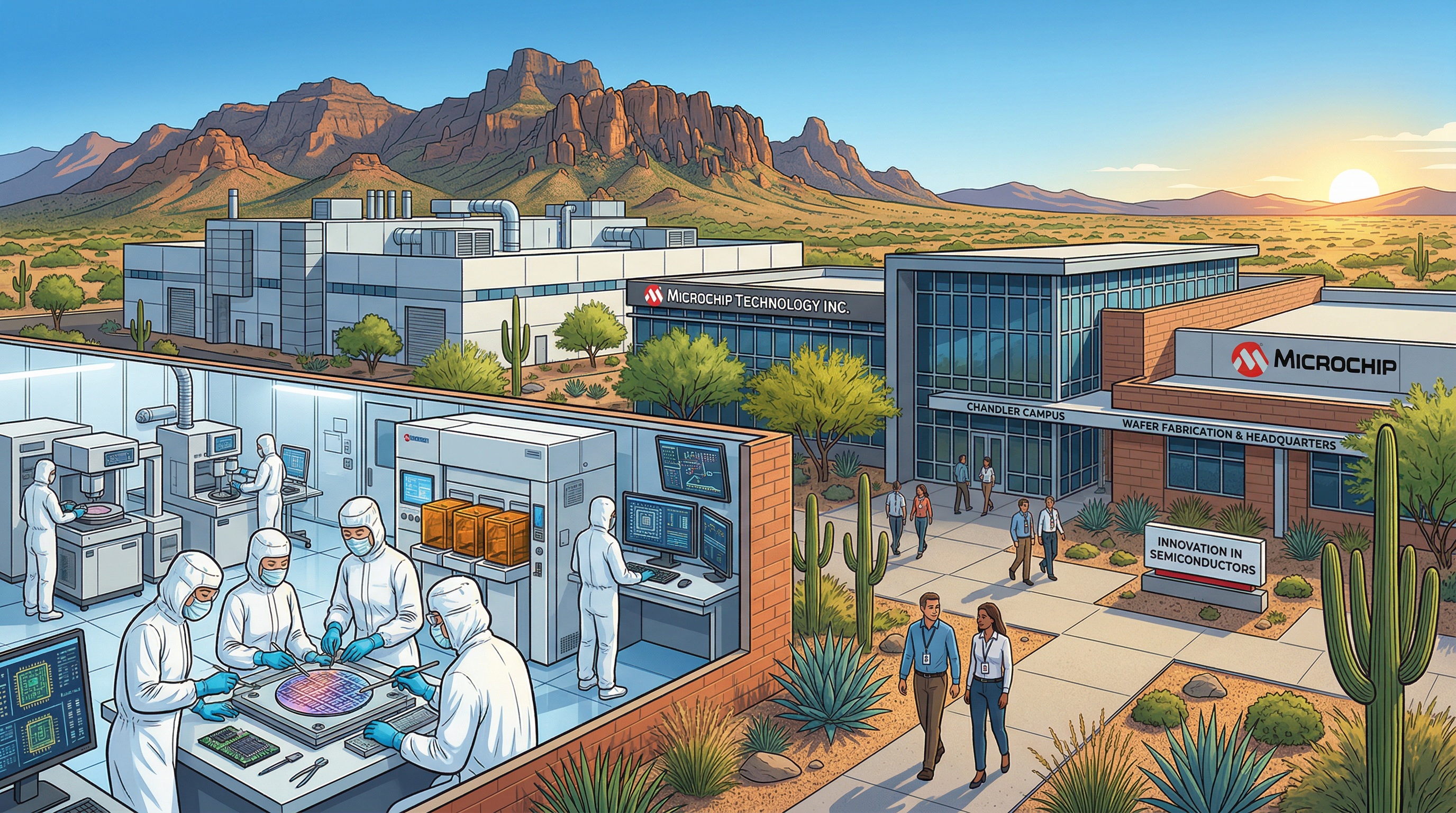
Microchip Technology
Chandler, AZ
Headquartered in Chandler. Designs and manufactures microcontrollers, FPGAs, and analog semiconductors. Operates its own fab in Tempe. Revenues over $7B annually.
🌵

Casa Grande: The Next Frontier

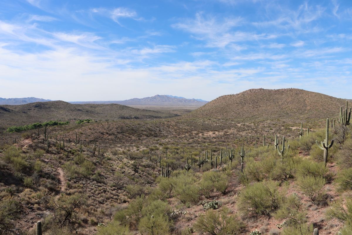
Casa Grande, located between Phoenix and Tucson, is emerging as Arizona's newest semiconductor corridor. The city's large available land parcels, proximity to I-10, water infrastructure investments, and competitive incentive packages are attracting fab-scale industrial development. Several major suppliers and back-end assembly operations have already announced or broken ground on facilities in the Casa Grande/Coolidge area, complementing the established Chandler and Tempe hubs to the north.

Why Arizona Leads

The factors behind Arizona's semiconductor dominance

CHIPS & Science Act Beneficiary

Arizona is the single largest recipient of CHIPS Act manufacturing incentives. TSMC received $6.6B in direct federal funding (plus $5B in loans) for its $165B North Phoenix campus. Intel received $8.5B for its Chandler Ocotillo campus. Total committed private investment in Arizona semiconductor manufacturing now exceeds $200 billion.

Established Semiconductor Corridor

The Chandler-Tempe-Phoenix corridor has hosted semiconductor manufacturing since the 1980s (Intel's first AZ fab opened 1981). Deep infrastructure, trained workforce, and supply chain already in place.

University Pipeline

Arizona State University, University of Arizona, and Maricopa Community Colleges produce thousands of engineering graduates annually. ASU has direct workforce development partnerships with TSMC and Intel.

Water & Power Infrastructure

Despite the desert environment, Arizona has invested heavily in reclaimed water systems for fab use. Salt River Project and APS provide reliable power, with chip fabs requiring up to 100MW each.

Supply Chain Ecosystem

Key suppliers including Entegris, Air Products, Edwards Vacuum, Linde, and dozens of specialty chemical companies have established Arizona operations to service the growing fab base.

National Security Rationale

Geopolitical diversification away from Taiwan concentration is a key driver. Arizona's fab expansion directly addresses the U.S. goal of producing 20% of leading-edge chips domestically by 2030.
An Immersive Journey

Inside the World's
Most Complex Process

From a grain of desert sand to a chip with 30 billion transistors — explore every step of semiconductor manufacturing at atomic scale.

Scale of this journey
1 m
1 nm
THE SCALE OF THIS JOURNEY
1 m Human Scale
300 mm Silicon Wafer
~7 mm Single Die
10 nm Transistor Pitch
2 nm Gate Length
0.28 nm Silicon Atom
STEP 01 Macro Scale

Sand & Silica Mining

The entire process begins with one of Earth's most abundant materials

7 companies involved
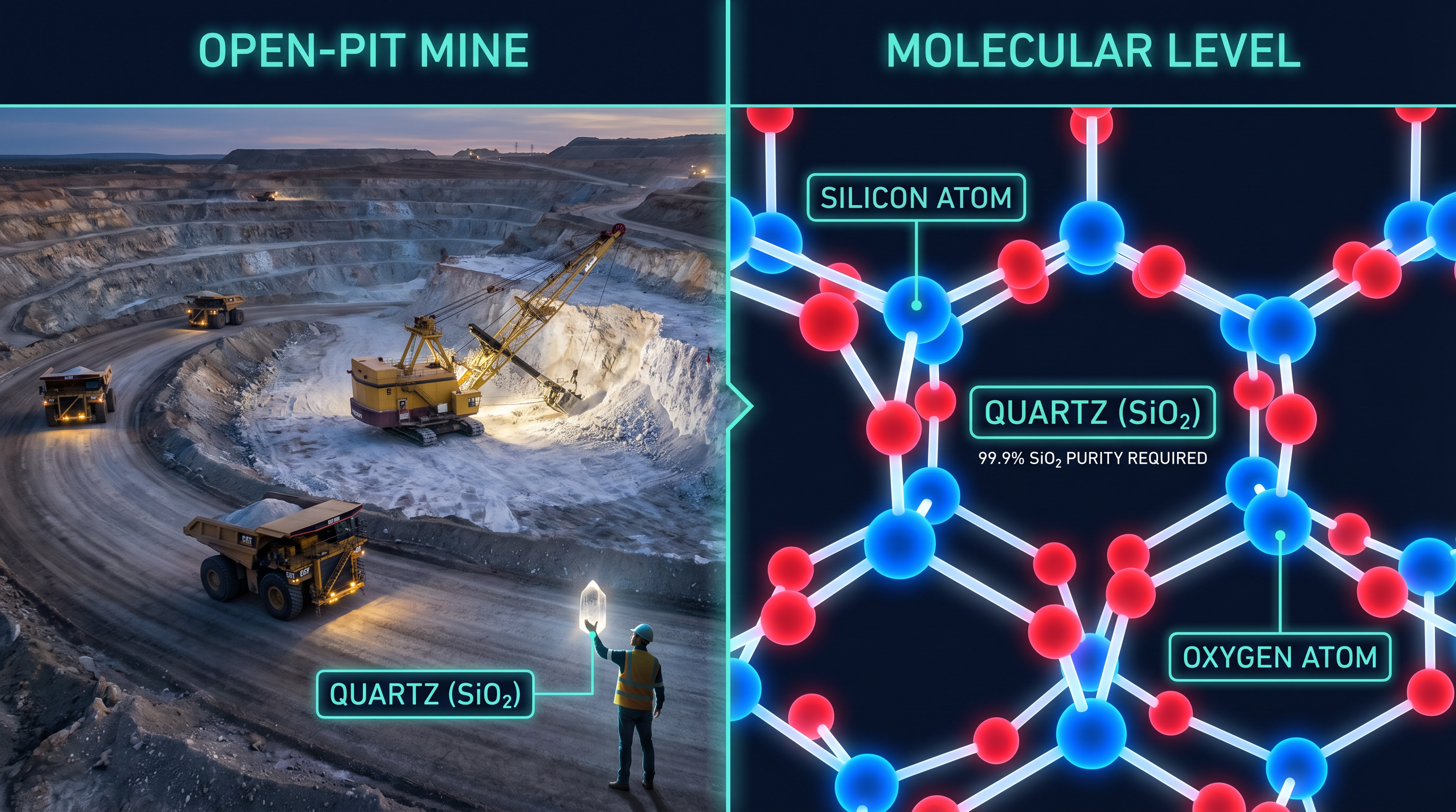
Sand and silica mining — open pit quartzite mine
MINE SCALE CHEMISTRY ATOMIC
The journey from sand to silicon chip begins in open-pit quartz mines. High-purity quartzite rock — silicon dioxide (SiO₂) — is blasted, crushed, and graded. The key requirement is purity: at least 99.9% SiO₂, with minimal iron, aluminum, and other trace metals. The largest deposits are found in Brazil, the US (Spruce Pine, NC), and Norway. A single 300mm wafer requires about 2 kilograms of refined quartz. The quartzite is then shipped to ferrosilicon smelters where the reduction process begins.

Key Stakeholders

Unimin/Sibelco The Quartz Corp (Spruce Pine) Ferroglobe Elkem Nordic Mining Superior Plus Energy REC Silicon feedstock division

Materials

Quartzite (SiO₂) Coke (carbon) Limestone Silica sand

Specifications

Purity required: ≥99.9% SiO₂  ·  Mine output: millions of tons/year
STEP 02 Macro / Chemical Scale

Silicon Purification — Metallurgical Grade

Sand is cooked into raw silicon at over 2,000°C

7 companies involved
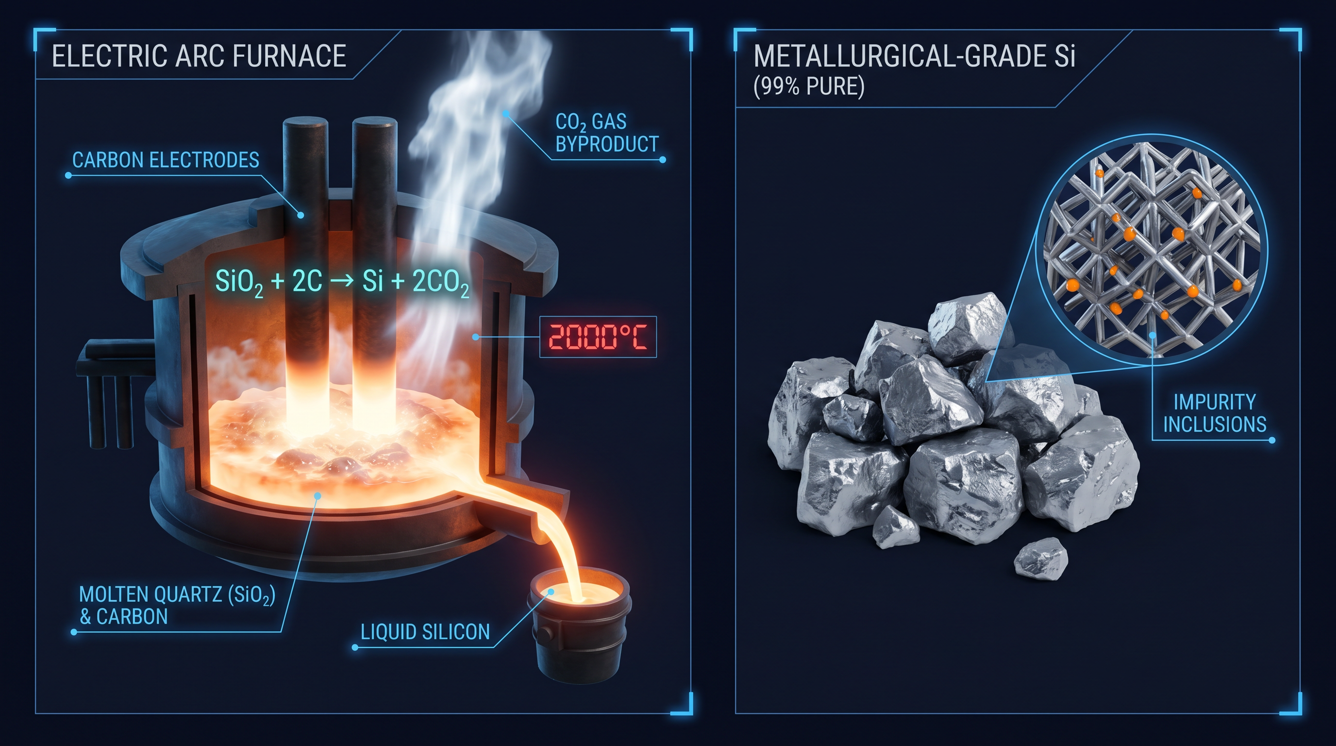
Submerged arc furnace smelting quartzite into metallurgical-grade silicon
INDUSTRIAL CHEMICAL MOLECULAR
Quartzite and carbon (coal/coke/woodchips) are loaded into a massive submerged-arc electric furnace. At temperatures exceeding 2,000°C, the carbon reduces the silicon dioxide: SiO₂ + 2C → Si + 2CO₂. The result is metallurgical-grade silicon (MG-Si) — about 98–99% pure. It's tapped from the furnace as a liquid and cast into chunks. This material is usable for solar cells and aluminum alloys, but it's still far too impure for semiconductors — which require 99.999999999% (eleven nines) purity. Further refining is essential.

Key Stakeholders

Ferroglobe Elkem Wacker Chemie REC Silicon Tokuyama Globe Specialty Metals Simcoa Operations

Materials

Quartzite (SiO₂) Petroleum coke Coal Woodchips Lime

Specifications

Temperature: 2,000°C  ·  Reaction: SiO₂ + 2C → Si + 2CO₂  ·  Purity: 98–99%
STEP 03 Molecular Scale

Polysilicon Production — Electronic Grade

Refined to 99.999999999% purity — cleaner than anything in nature

8 companies involved
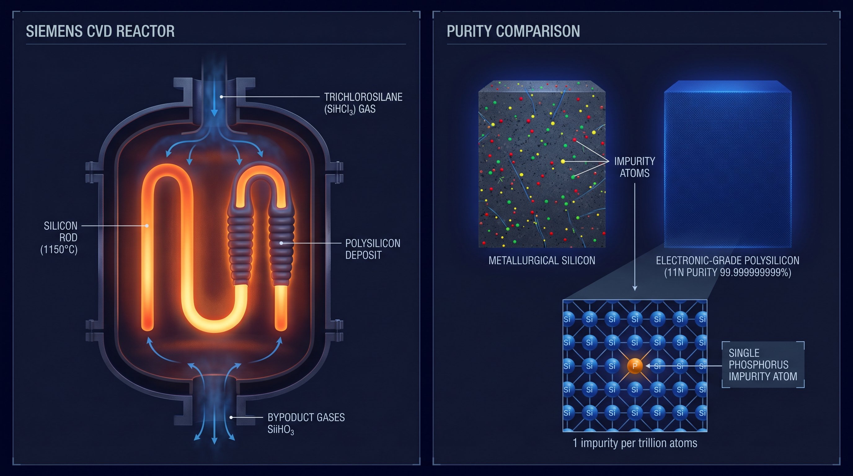
Siemens CVD reactor producing electronic-grade polysilicon rods
INDUSTRIAL CHEMICAL MOLECULAR
Metallurgical-grade silicon is converted to trichlorosilane gas (SiHCl₃) by reacting with HCl. This gas is purified by fractional distillation — chemical distillation removes virtually all impurities. The purified trichlorosilane is then fed into a Siemens CVD reactor: slim silicon rods are heated to 1,150°C and the gas decomposes, depositing layer upon layer of ultra-pure polysilicon onto the rods. The process takes days. The result: polysilicon rods of 11N purity — just one impurity atom per trillion silicon atoms. This is arguably the purest manufactured material on Earth.

Key Stakeholders

Wacker Chemie Hemlock Semiconductor OCI Company REC Silicon GCL-Poly Tokuyama Daqo New Energy Asia Silicon

Materials

Metallurgical Si HCl gas Trichlorosilane (SiHCl₃) H₂ gas

Specifications

Purity: 99.999999999% (11N)  ·  Reactor temp: 1,150°C  ·  Duration: 50–100 hours
STEP 04 Atomic Scale

Crystal Growth — Czochralski Process

Molten silicon pulled into a flawless single crystal

8 companies involved
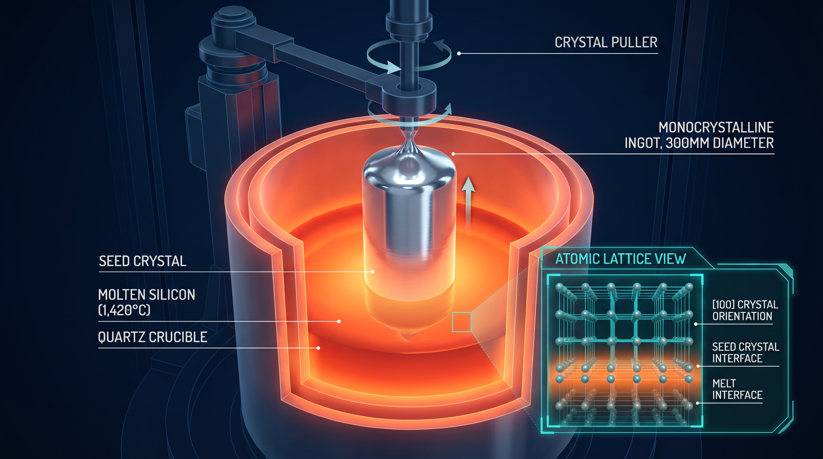
Czochralski crystal growth — pulling a monocrystalline silicon ingot from molten silicon
INDUSTRIAL CHEMICAL ATOMIC Lattice
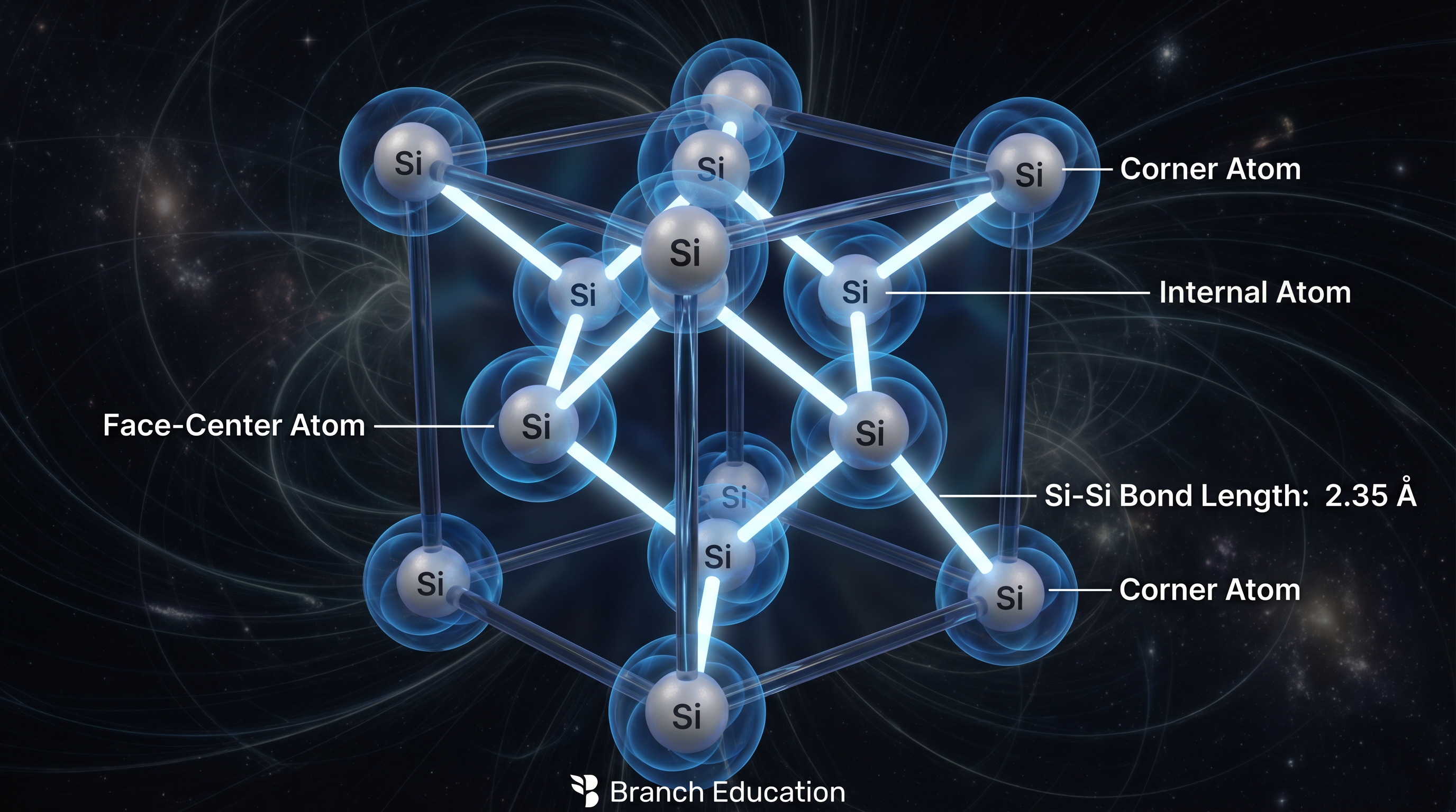
Polysilicon chunks are loaded into a quartz crucible and melted at 1,420°C — just above silicon's melting point. A tiny seed crystal on a rotating rod is lowered until it touches the melt surface. As it's slowly pulled upward at ~1mm/hour while rotating, silicon atoms from the melt lock onto the seed's crystal lattice in perfect alignment. The result: a monocrystalline silicon cylinder (ingot) up to 2 meters long and 300mm wide — every atom aligned in the same diamond cubic structure. A precisely controlled amount of dopant (boron or phosphorus) is added to the melt to set the wafer's base conductivity type. One misaligned atom can destroy a wafer.

Key Stakeholders

Shin-Etsu Chemical Sumco Corp GlobalWafers Siltronic SK Siltron Ferrotec Virginia Semiconductor Okmetic

Materials

Electronic-grade polysilicon Seed crystal Quartz crucible Argon gas Boron/Phosphorus dopant

Specifications

Melt temperature: 1,420°C  ·  Pull rate: ~1mm/hour  ·  Ingot: 300mm Ø × 2m long
STEP 05 Macro / Micro Scale

Ingot Slicing & Wafer Polishing

Diamond wire saws cut the ingot into mirror-smooth discs

8 companies involved
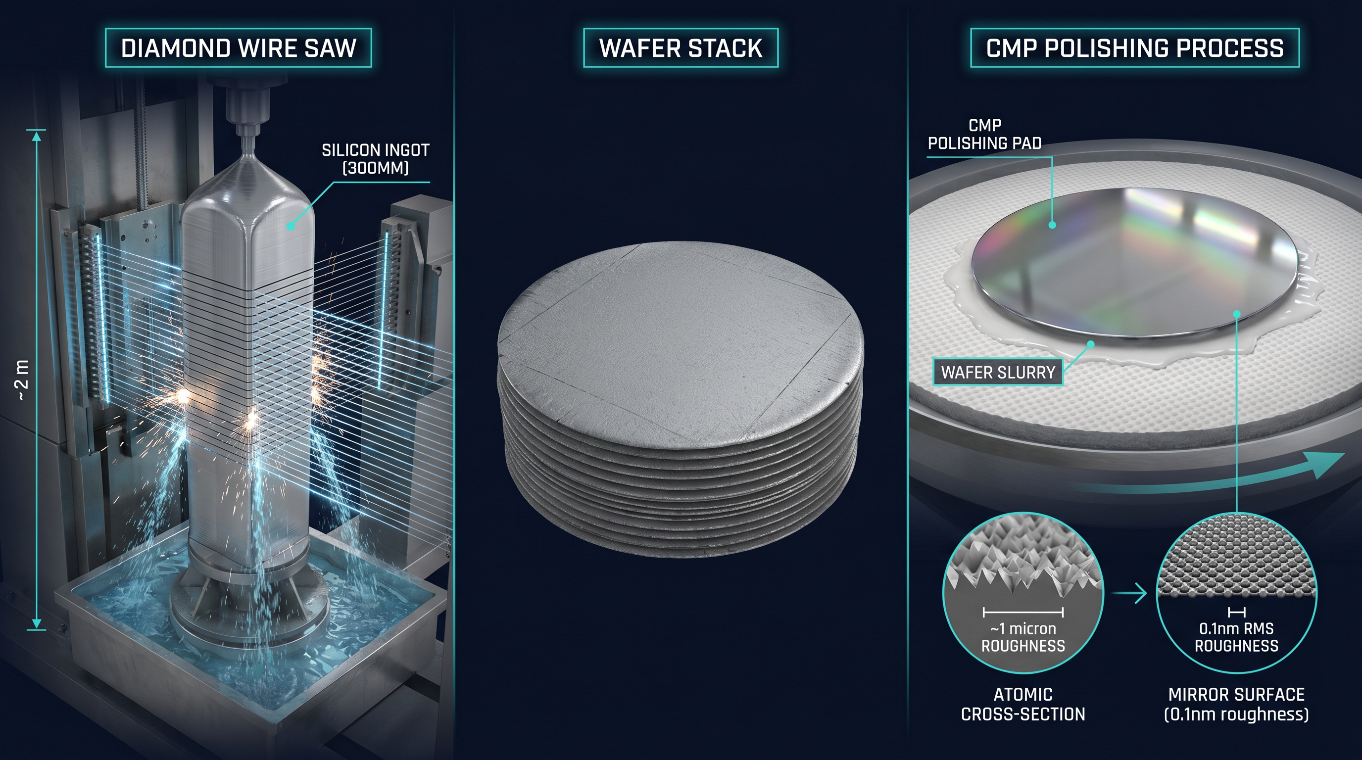
Diamond wire saw slicing silicon ingot into wafers
MACRO MICRO ATOMIC
The ingot is first ground to a precise 300mm diameter and given a flat notch indicating crystal orientation. It's then mounted in a multi-wire saw: hundreds of parallel diamond-coated wires run at high speed through the ingot, slicing it into 0.775mm-thick wafers simultaneously. Each wafer is then lapped, acid-etched to remove saw damage, polished with colloidal silica (CMP) to a mirror finish, and cleaned in an ultra-pure water rinse. The final wafer surface roughness is less than 0.1nm RMS — flatter and smoother than any natural surface. Each finished wafer is inspected for particles, crystal defects, and geometry before use.

Key Stakeholders

Shin-Etsu Chemical Sumco GlobalWafers Siltronic SK Siltron Disco Corp (wire saws) Meyer Burger Komatsu Electronic Metals

Materials

Silicon ingot Diamond wire Lapping slurry HF/HNO₃ etch Colloidal silica CMP slurry

Specifications

Wafer thickness: 0.775mm  ·  Surface roughness: <0.1nm RMS  ·  Diameter: 300mm
STEP 06 Design Scale (nm on paper)

Chip Architecture & Design — EDA

Engineers map billions of transistors before a single wafer is touched

6 companies involved
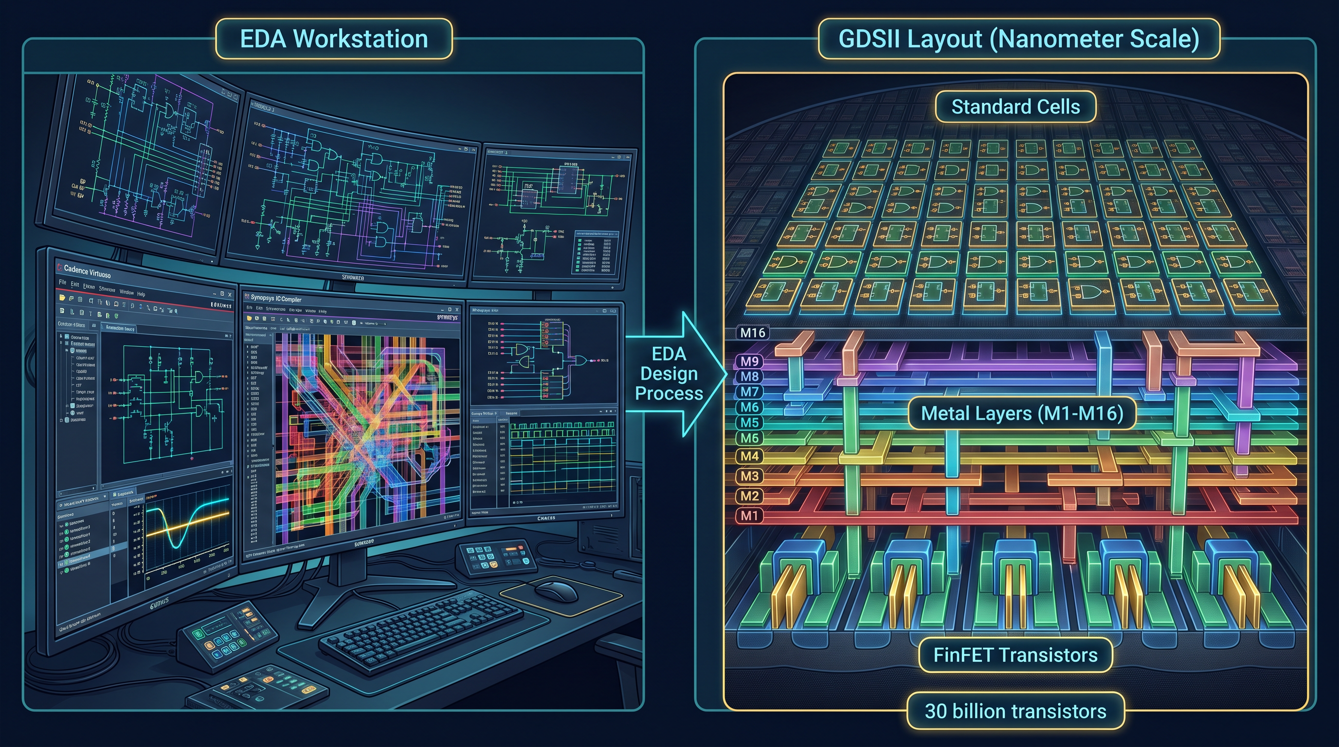
Electronic design automation — chip layout on EDA software showing transistor placement
SYSTEM 💻 Logic Design PHYSICAL nm
A modern chip like Apple's M4 or NVIDIA's H100 contains over 80 billion transistors — all designed on computers before manufacturing begins. Chip architects define the logic blocks, memory hierarchies, and interconnects at the RTL (Register Transfer Level) in VHDL or Verilog code. EDA (Electronic Design Automation) software then synthesizes this into a gate-level netlist, places millions of standard cells, and routes copper wires across 16+ metal layers. The final GDSII file — the chip's "blueprint" — is terabytes in size. Timing analysis ensures every signal meets its deadline at 4GHz+. A single chip design team can have 1,000+ engineers and take 3–5 years.

Key Stakeholders

Synopsys Cadence Design Systems Siemens EDA (Mentor) ANSYS (chip simulation) ARM Holdings (IP) Keysight Silvaco OpenROAD SEMI standard bodies

Materials

EDA software licenses Server farms IP blocks Standard cell libraries

Specifications

Design time: 3–5 years  ·  Engineers: 500–2,000  ·  GDSII file: 1–10 TB
STEP 07 Nanometer Scale

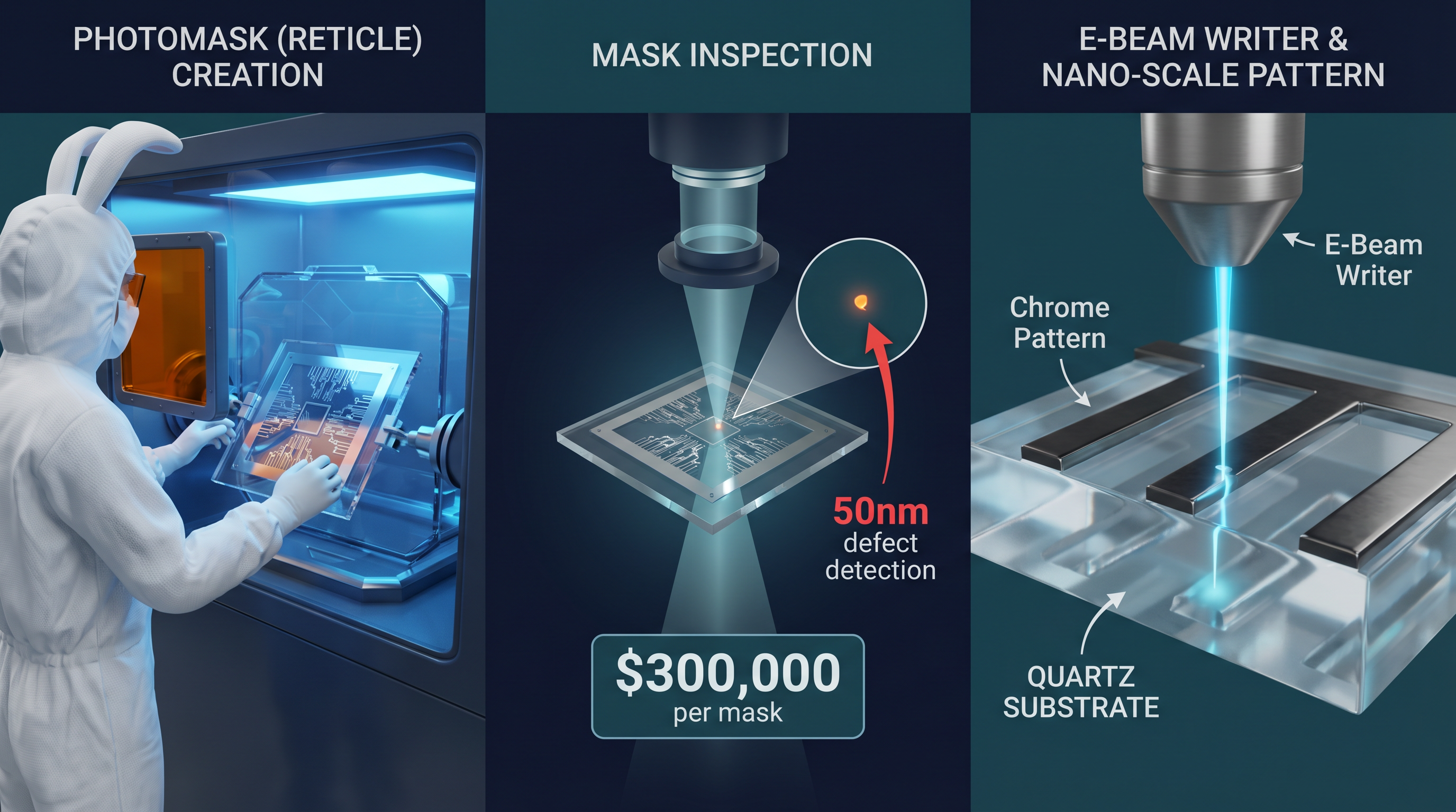
Photomask Creation

Glass plates etched with circuit patterns — each one worth $300,000

7 companies involved
Photomask — electron beam written quartz glass mask with nanometer circuit patterns
LAB NANO ATOMIC
The GDSII chip design data is used to create photomasks — ultra-flat 6-inch quartz glass plates with chrome circuit patterns. An e-beam (electron beam) writer draws the patterns at nanometer precision: this takes 12–24 hours per mask. The chrome is etched away where the electron beam exposed the resist, leaving an opaque/transparent pattern. Each mask layer is then inspected by dedicated systems scanning for defects as small as 20nm. A full chip set requires 50–80 unique masks. Each EUV mask costs ~$300,000. If a mask is defective, it must be repaired or scrapped — mask quality directly determines chip yield.

Key Stakeholders

Photronics Toppan Photomasks Hoya DNP (Dai Nippon Printing) SK Electronics Zeiss (mask inspection) KLA (mask inspection) NuFlare (e-beam writers)

Materials

Quartz glass substrate Chrome layer E-beam resist Chromium etchant

Specifications

E-beam write time: 12–24 hrs/mask  ·  Defect spec: <20nm  ·  Cost: ~$300K/mask  ·  Full set: 50–80 masks
STEP 08 Atomic Scale — 2nm layer

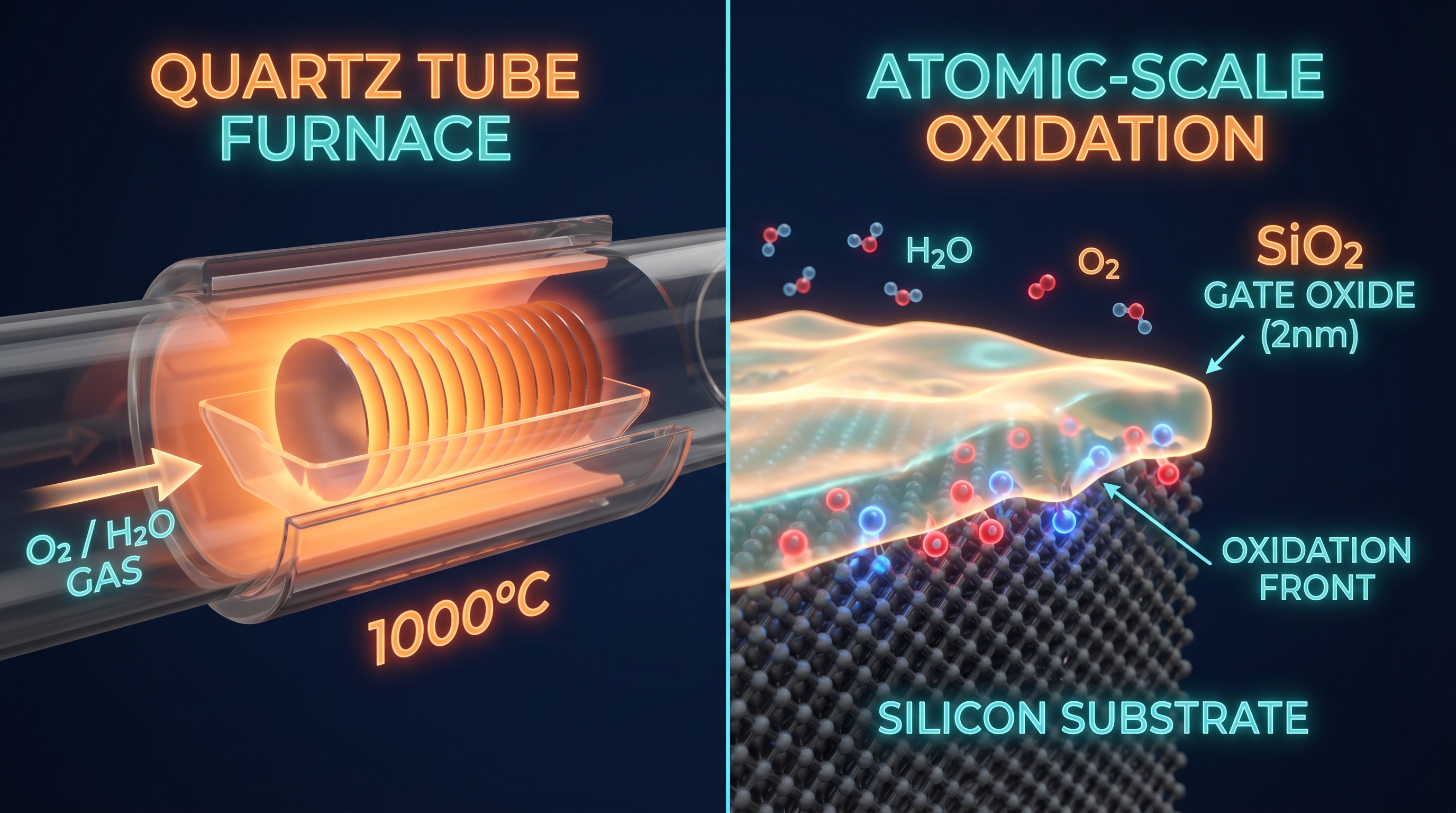
Thermal Oxidation

The wafer is baked in oxygen to grow a nanometer-thin insulating shield

7 companies involved
Thermal oxidation furnace — silicon wafers oxidizing in a quartz tube at 1000°C
FURNACE NANO ATOMIC
Silicon wafers are loaded into a quartz tube furnace at 800–1,100°C in an atmosphere of pure oxygen or steam. Silicon atoms at the surface react with oxygen to form silicon dioxide (SiO₂) — the same glass-like material as quartz. This oxide grows from the surface inward, consuming silicon. At 1,000°C in dry O₂, it grows at about 1nm/minute. The resulting SiO₂ is an extraordinary insulator with a breakdown field of 10MV/cm. It forms the gate dielectric in transistors — the critical 1–2nm layer between the gate electrode and the silicon channel. This step is repeated multiple times throughout the fab process to form different oxide layers.

Key Stakeholders

Applied Materials (furnace systems) Tokyo Electron (TEL) Kokusai Electric ASM International Lam Research Centrotherm Tempress Systems

Materials

Silicon wafer O₂ gas (dry oxidation) H₂O vapor (wet oxidation) N₂ purge gas

Specifications

Temperature: 800–1,100°C  ·  Growth rate: 1nm/min (dry O₂)  ·  Gate oxide: 1–2nm  ·  Breakdown: 10MV/cm
STEP 09 Atomic Scale — monolayers

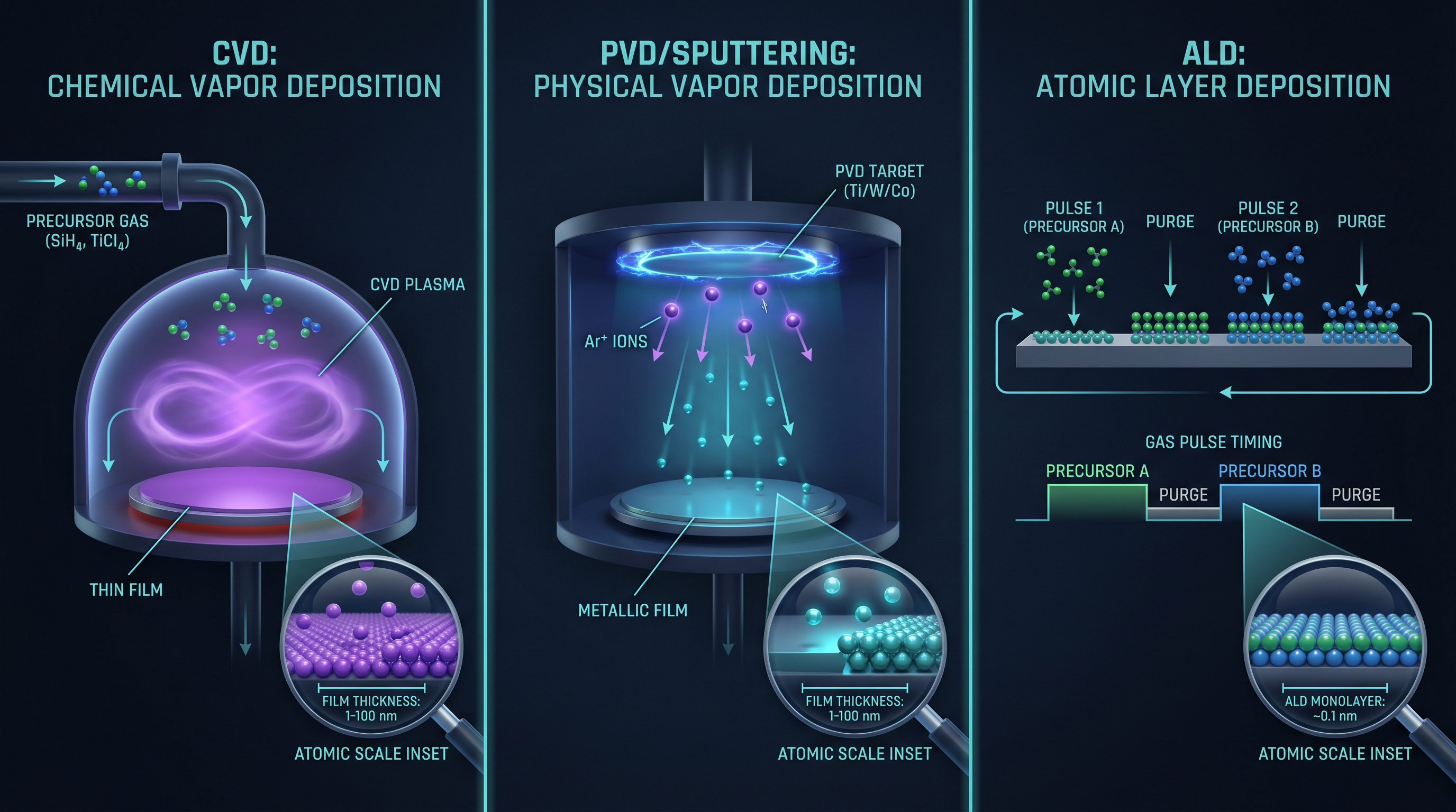
Thin Film Deposition — CVD / PVD / ALD

Layers of material just atoms thick are deposited one by one

8 companies involved
CVD/ALD deposition chamber — atomic layer deposition of thin films on silicon wafer
CHAMBER NANO Monolayer
Building the chip's layers requires depositing many different materials — silicon nitride, silicon dioxide, titanium nitride, tungsten, copper — at precise thicknesses down to a single atomic monolayer. Three techniques: CVD (Chemical Vapor Deposition) — precursor gases react in plasma to deposit films; PVD/Sputtering — argon plasma bombards a metal target, ejecting atoms that coat the wafer; ALD (Atomic Layer Deposition) — self-limiting surface reactions deposit exactly one monolayer per cycle (0.1nm), allowing atomic-level thickness control. A leading-edge chip involves 300+ deposition steps. Applied Materials and Lam Research dominate this equipment market.

Key Stakeholders

Applied Materials Lam Research ASM International Tokyo Electron Kokusai Electric Jusung Engineering Wonik IPS Aixtron

Materials

SiH₄ (silane) TiCl₄ NH₃ WF₆ Al(CH₃)₃ (TMA) Ar gas N₂ gas

Specifications

ALD thickness: 0.1nm/cycle  ·  CVD rate: 1–10 nm/min  ·  Temperature: 300–700°C
STEP 10 Nanometer Scale

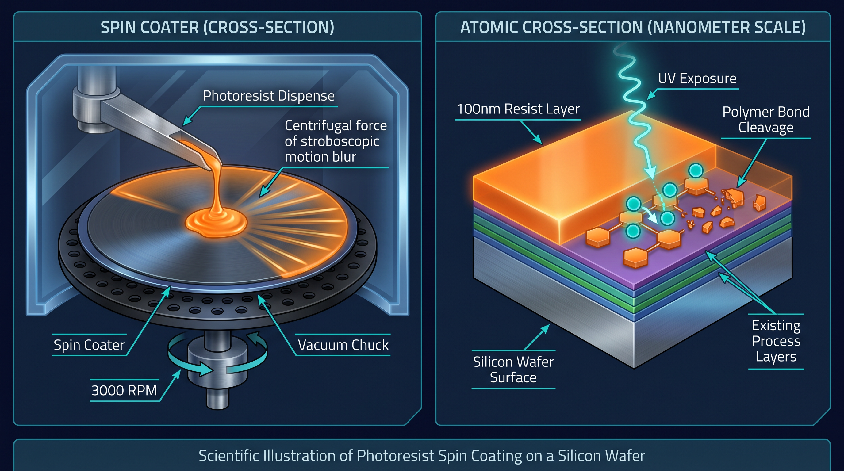
Photoresist Coating

A light-sensitive chemical is spun across the wafer surface

7 companies involved
Photoresist spin coating — centrifugal force spreading light-sensitive polymer across wafer
Track Tool NANO Film Polymer Chain
The wafer is first treated with HMDS adhesion promoter, then placed on a spin coater — a vacuum chuck that spins at 1,500–4,000 RPM. A few milliliters of liquid photoresist are dispensed at center; centrifugal force spreads it into a perfectly uniform 50–200nm thin film. The wafer is then baked on a hot plate (90°C) to drive off solvent. Photoresist is a light-sensitive polymer: in positive resist (used for most leading-edge nodes), EUV or DUV photons break the polymer chains in exposed areas, making them soluble in developer. In negative resist, exposure crosslinks the polymer, making unexposed areas soluble. The photoresist thickness, uniformity, and adhesion directly impact lithography resolution.

Key Stakeholders

JSR Corporation Tokyo Ohka Kogyo (TOK) Shin-Etsu Chemical DuPont Merck KGaA Fujifilm Electronic Materials Dongjin Semichem

Materials

Photoresist (CAR) HMDS adhesion promoter PGMEA solvent Developer (TMAH)

Specifications

Spin speed: 1,500–4,000 RPM  ·  Thickness: 50–200nm  ·  Uniformity: ±2%  ·  Bake: 90°C
STEP 11 7nm–13nm

Photolithography — EUV / DUV

Extreme ultraviolet light prints circuit patterns smaller than a virus

8 companies involved
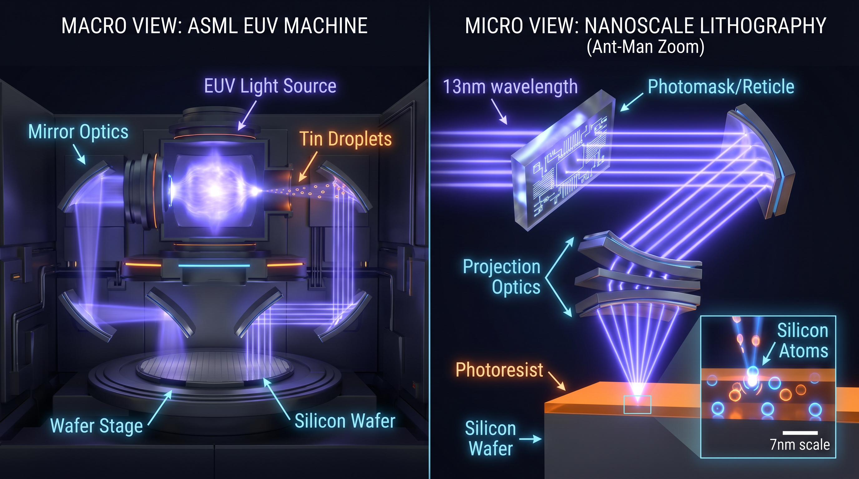
ASML EUV scanner — extreme ultraviolet lithography printing nanoscale circuits onto silicon wafer
Scanner EUV 13.5nm Photon
The most critical and expensive step in chip manufacturing. An ASML NXE EUV scanner fires a 50kW CO₂ laser at tin droplets 50,000 times per second, generating plasma that emits 13.5nm extreme ultraviolet light. This light is shaped by 11 ultra-precise molybdenum/silicon multilayer mirrors (made by Zeiss) and shone through the photomask. The optics reduce the image 4× and project it onto the photoresist-coated wafer. The stage moves to each die position with sub-nanometer precision. One ASML EUV NXE:3600D machine costs $380 million, weighs 180 tons, and ships in 40 freight containers. Each wafer visits the lithography cluster ~80 times during fabrication. The lines drawn are 10nm wide — 45 silicon atoms across.

Key Stakeholders

ASML TSMC Samsung Foundry Intel Foundry SK Hynix Zeiss (optics) JSR (resist) Entegris (filtration) Cymer (light source)

Materials

EUV photons (13.5nm) Tin (Sn) droplets CO₂ drive laser Chemically amplified resist Photomask ($300K)

Specifications

Wavelength: 13.5nm  ·  Machine cost: $380M  ·  Weight: 180 tons  ·  Overlay accuracy: <2nm  ·  Throughput: 160 wafers/hour
STEP 12 Nanometer Scale

Etching

Chemicals or plasma carve the exposed circuit pattern into the wafer

8 companies involved
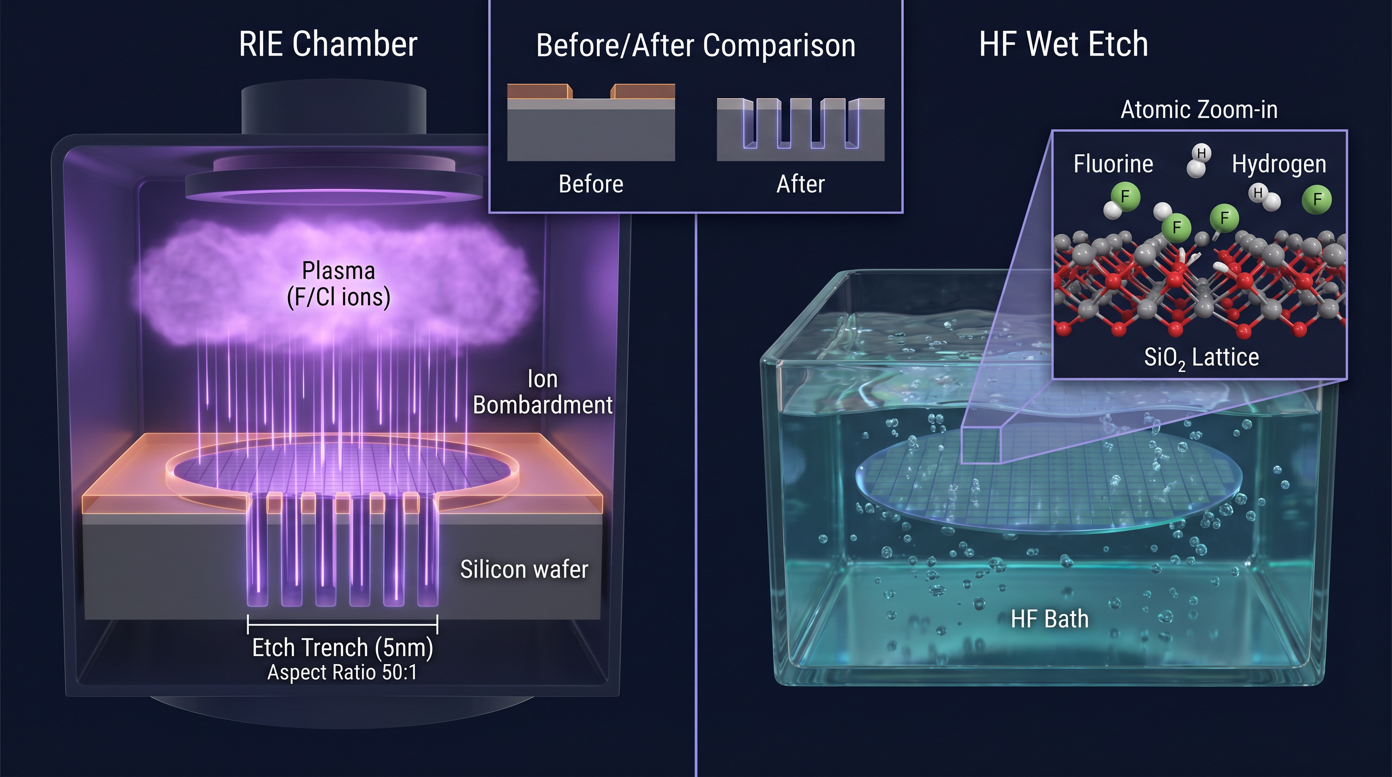
Reactive ion etching — plasma carving nanoscale circuit features into silicon wafer
CHAMBER Plasma ATOMIC Layer
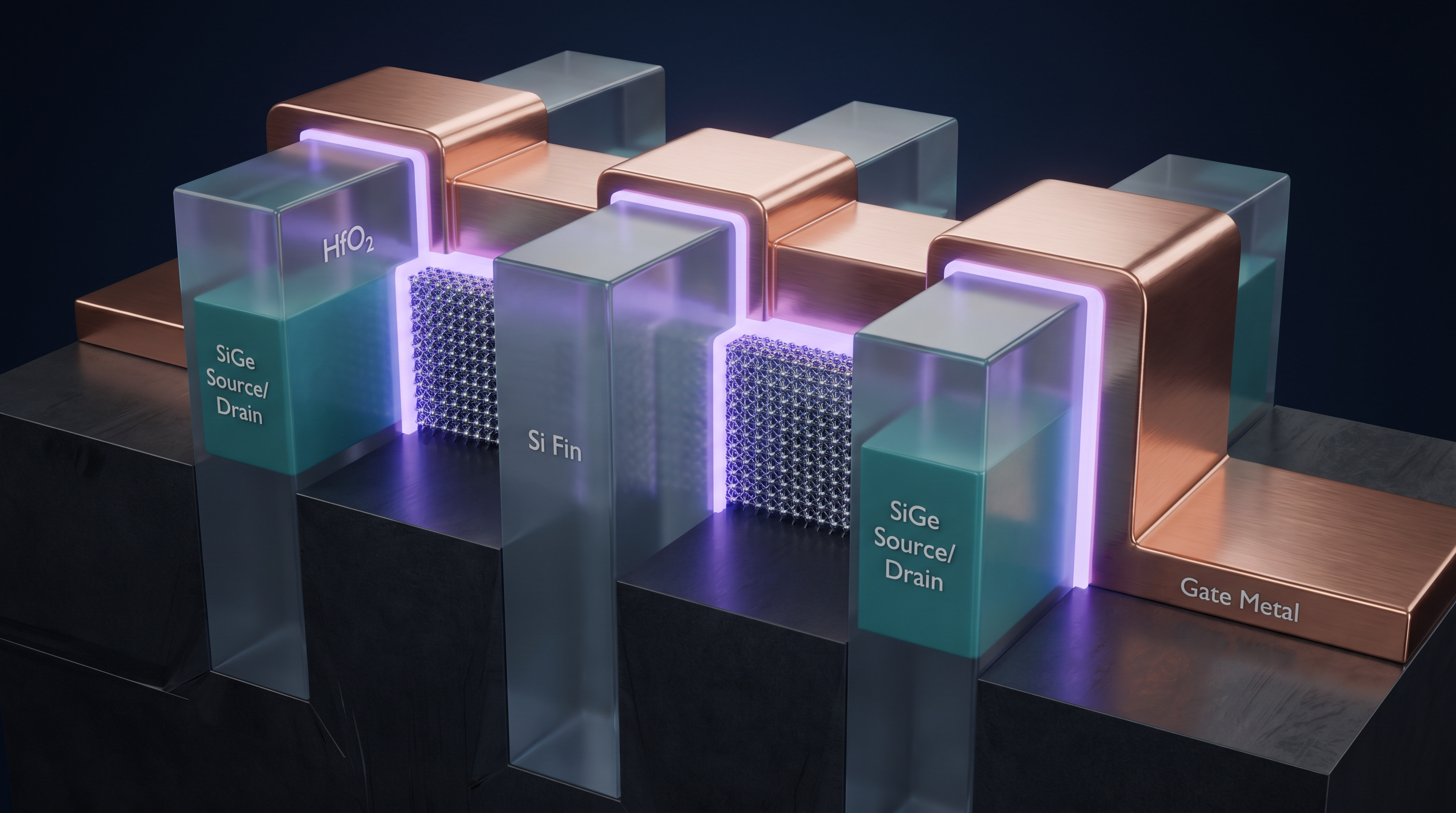
After lithography exposes the photoresist, etching transfers the pattern into the underlying material. Dry etching (Reactive Ion Etching / RIE) uses fluorine, chlorine, or bromine plasma to etch silicon, silicon nitride, or metals with extreme directionality — creating vertical sidewalls with aspect ratios up to 100:1 in memory devices. Atomic Layer Etching (ALE) removes material exactly one atomic layer at a time for the most precise nodes. Wet etching uses liquid chemicals (HF for SiO₂, KOH for Si, H₃PO₄ for SiN) for less critical steps. Etch selectivity — etching one material without touching another — is the key challenge. A 2nm node FinFET gate has tolerances of ±0.5nm.

Key Stakeholders

Lam Research Applied Materials Tokyo Electron Hitachi High-Tech Oxford Instruments Plasma-Therm SPTS Technologies Mattson Technology

Materials

CF₄/CHF₃/C₄F₈ (oxide etch) Cl₂/HBr (poly-Si etch) SF₆ (Si etch) HF (wet oxide etch)

Specifications

RIE aspect ratio: up to 100:1  ·  ALE precision: 1 atomic layer  ·  Selectivity: >100:1 Si:SiO₂
STEP 13 10–100nm junction depth

Ion Implantation & Doping

Atoms are fired at near-light speed to alter silicon's conductivity

7 companies involved
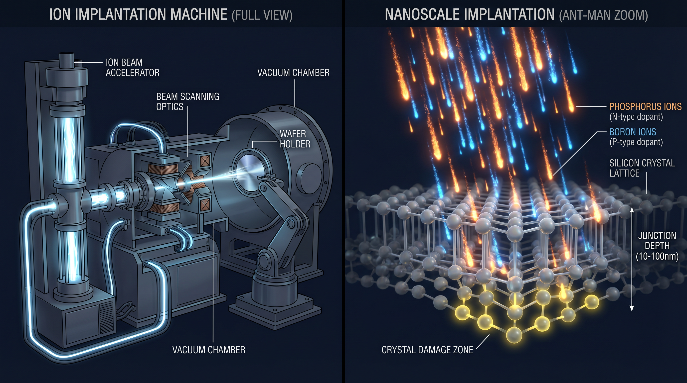
Ion implantation — high-energy ion beam firing dopant atoms into silicon wafer
Implanter Junction Ion
Transistors work by creating regions of opposite electrical polarity in silicon — N-type (electron-rich) and P-type (electron-poor). This is done by ion implantation: phosphorus or arsenic atoms (N-type) and boron atoms (P-type) are ionized, accelerated to energies of 1 keV–3 MeV, and fired into the silicon wafer at precise depths. At 3 MeV, ions enter the silicon at ~5% the speed of light. The ion beam is scanned across the wafer with precision positioning. Implant doses range from 10¹⁰ to 10¹⁶ ions/cm². Only about 1 dopant atom per 10,000 silicon atoms is needed to completely alter the material's conductivity. The crystal is damaged by the ion impacts — this is repaired in the next step.

Key Stakeholders

Applied Materials (VIISta) Axcelis Technologies Nissin Ion Equipment Sumitomo Heavy Industries Kyocera Advanced Energy Industries MKS Instruments

Materials

Phosphorus ions (PH₃) Boron ions (BF₃) Arsenic ions (AsH₃) Helium/H₂ (beam transport)

Specifications

Energy: 1 keV–3 MeV  ·  Junction depth: 10–100nm  ·  Ion speed: up to 5% c  ·  Dose: 10¹⁰–10¹⁶ cm⁻²
STEP 14 Atomic Scale

Rapid Thermal Annealing

A millisecond flash of heat repairs the crystal and activates dopants

6 companies involved
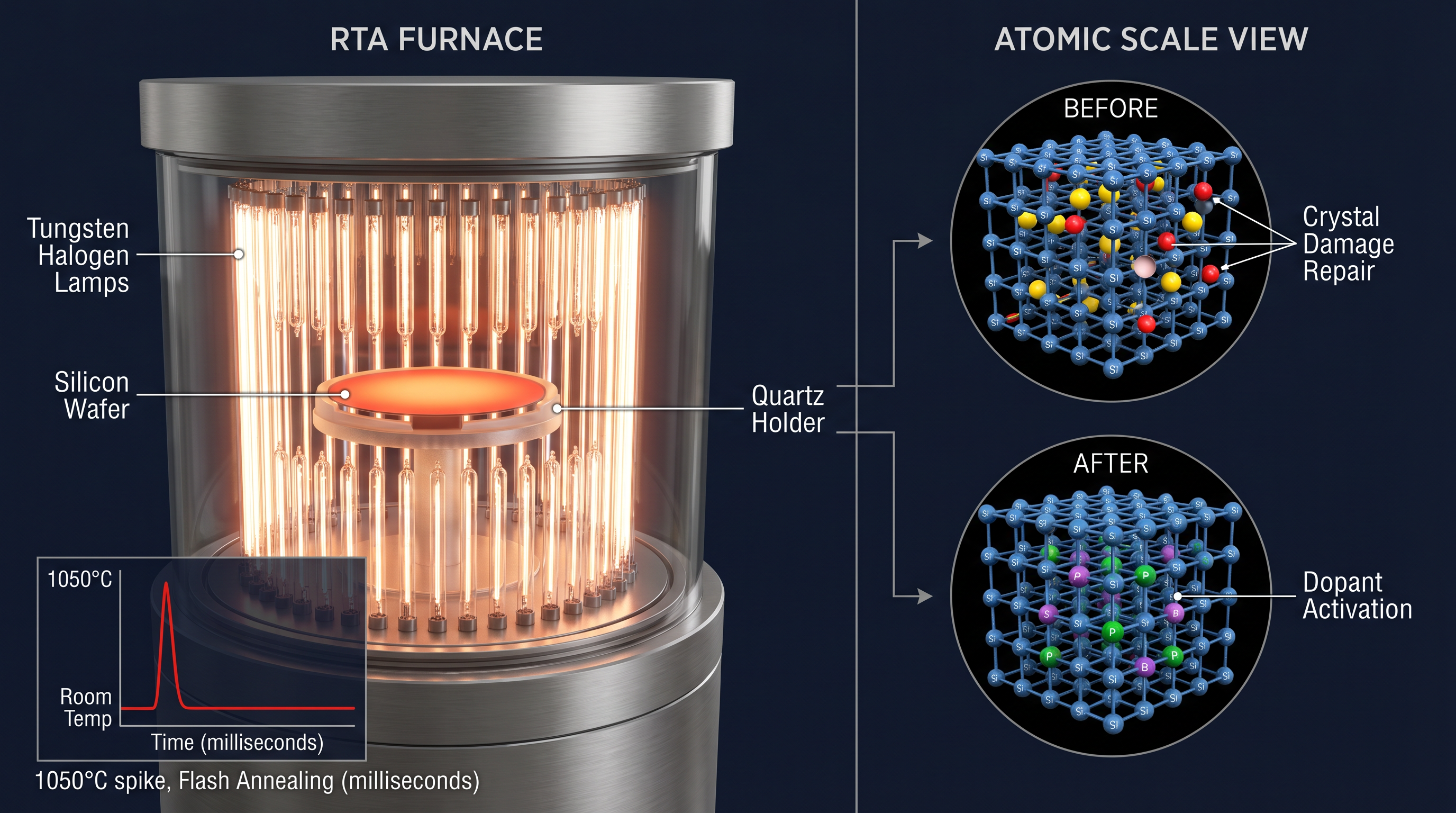
Rapid thermal processing — tungsten halogen lamps flash heating silicon wafer for crystal annealing
RTP Chamber CRYSTAL Lattice Repair
Ion implantation leaves the silicon crystal severely damaged — silicon atoms are knocked out of their lattice positions, creating vacancies and interstitials. The dopant atoms are also sitting in interstitial positions where they're electrically inactive. Rapid Thermal Processing (RTP) fixes both problems: the wafer is heated from room temperature to 1,050°C in under 1 second using banks of tungsten-halogen lamps, held for 1–10 seconds, then cooled. The brief, intense heat allows silicon atoms to diffuse back into lattice sites (annealing the crystal), while dopant atoms move into substitutional positions (activating them). Flash Lamp Annealing (FLA) uses millisecond pulses for even less thermal budget — critical for sub-5nm nodes where dopant diffusion of even 1nm would destroy the transistor.

Key Stakeholders

Applied Materials (Vantage RTP) Mattson Technology Screen Semiconductor Solutions Ultratech (now Veeco) Kokusai Electric AXT Inc Therco Systems

Materials

Tungsten halogen lamps Pyrometer (temp sensor) N₂ ambient

Specifications

Peak temp: 950–1,100°C  ·  Ramp rate: 200°C/sec  ·  Duration: milliseconds to 10 seconds
STEP 15 Atomic Scale Flatness

Chemical Mechanical Planarization — CMP

The wafer surface is polished flat to within a single atom's height

7 companies involved
CMP polishing tool — wafer pressed against rotating polishing pad with slurry for planarization
Polish Tool Surface 1nm Flat
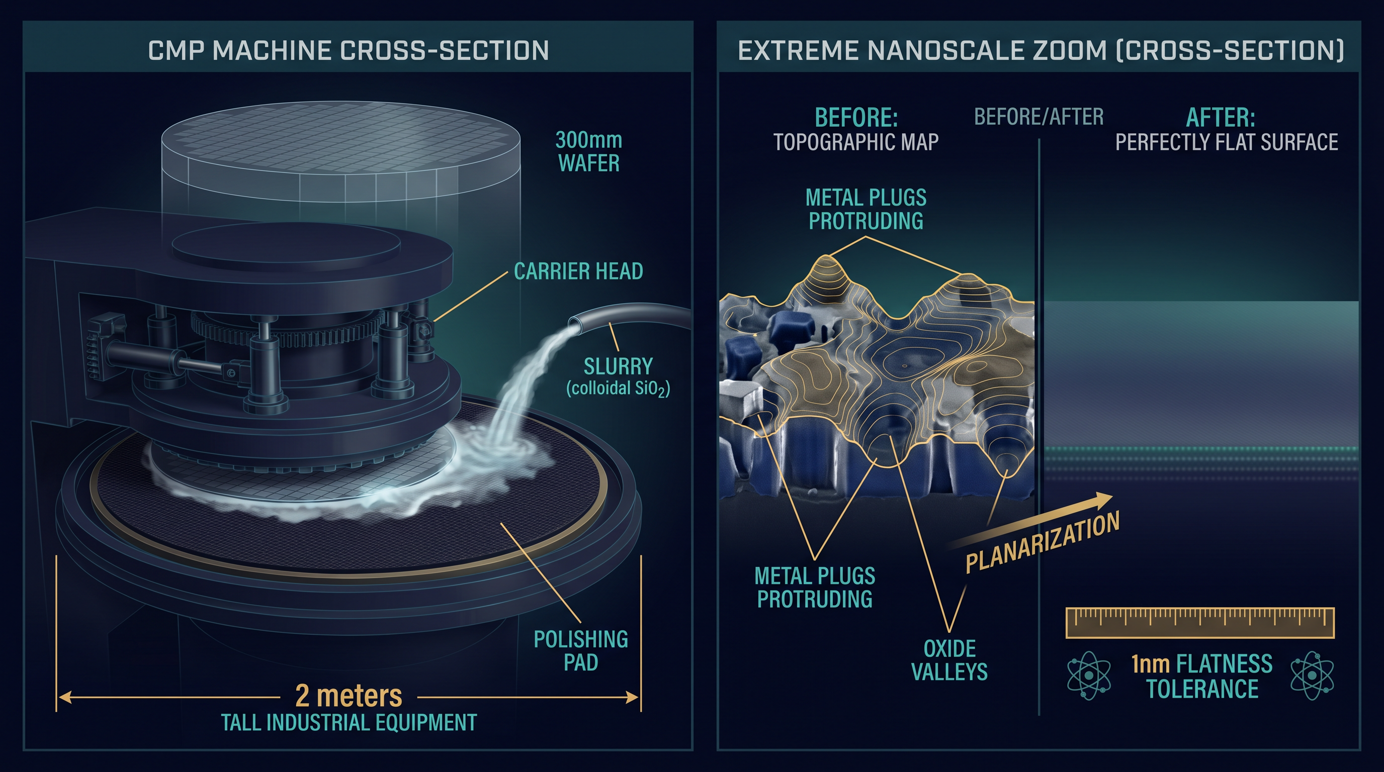
As layers are built up on the wafer, the surface becomes increasingly rough and non-planar — oxide steps, metal plugs, trench fills all create topology. CMP (Chemical Mechanical Planarization) uses a combination of chemistry and abrasion to create a perfectly flat surface for the next layer. The wafer is pressed face-down against a rotating polyurethane polishing pad, with colloidal silica (50–200nm particles suspended in alkaline slurry) flowing between them. The chemistry softens the high spots while mechanical abrasion removes them. After CMP, the surface is flat to within 1nm across the entire 300mm wafer. A leading-edge chip requires 15–20 CMP steps. Each step must remove exactly the right amount — too little leaves bumps, too much damages the layer below.

Key Stakeholders

Applied Materials (Reflexion GT) Ebara KLA (post-CMP inspection) Entegris (slurry) CMC Materials Fujimi (slurry) Cabot Microelectronics Nihon Cabot

Materials

Colloidal silica slurry Ceria (CeO₂) slurry H₂O₂ oxidizer Polyurethane polishing pad

Specifications

Flatness: <1nm  ·  Material removal: 50–500nm/step  ·  Uniformity: ±3% across 300mm wafer
STEP 16 Nanometer Scale

Metallization & Copper Interconnects

Copper wiring connects every transistor across 16 stacked layers

8 companies involved
Copper interconnects — dual damascene process building multi-layer copper wiring network
Plating Tool 12nm Wire ATOMIC
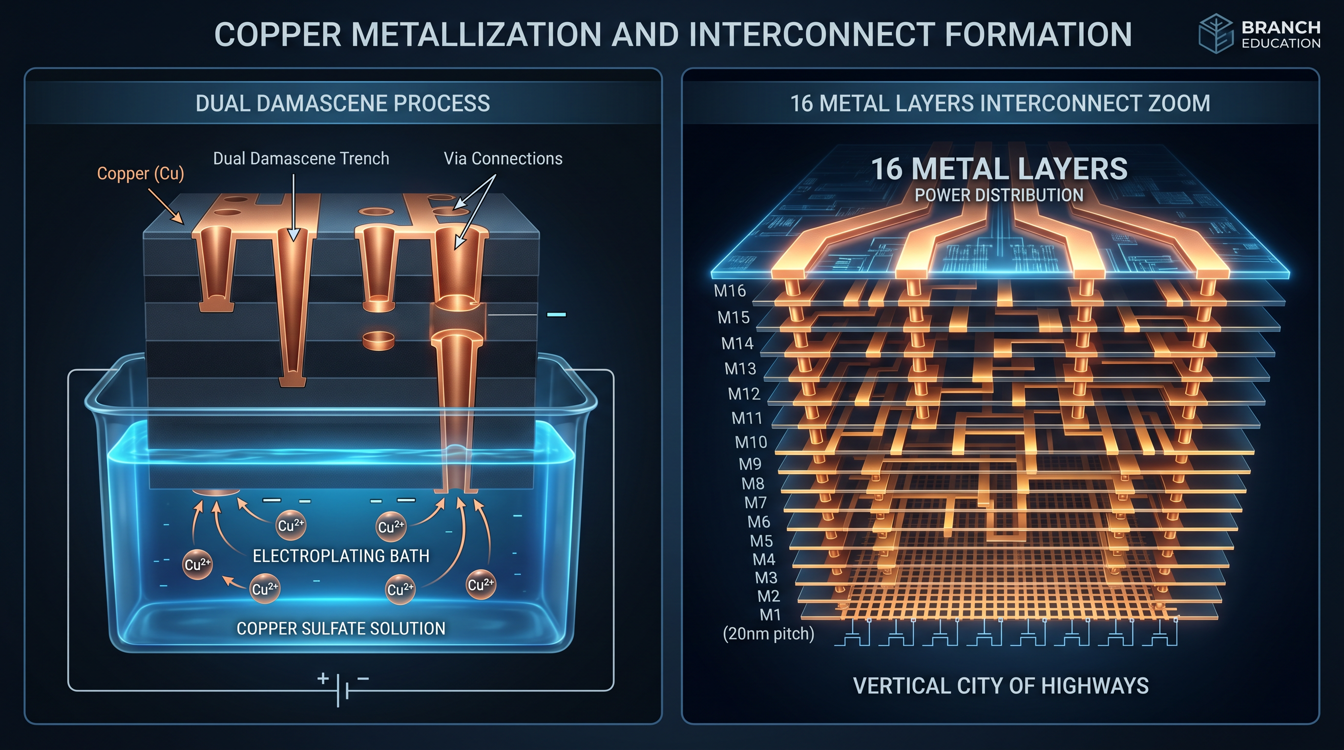
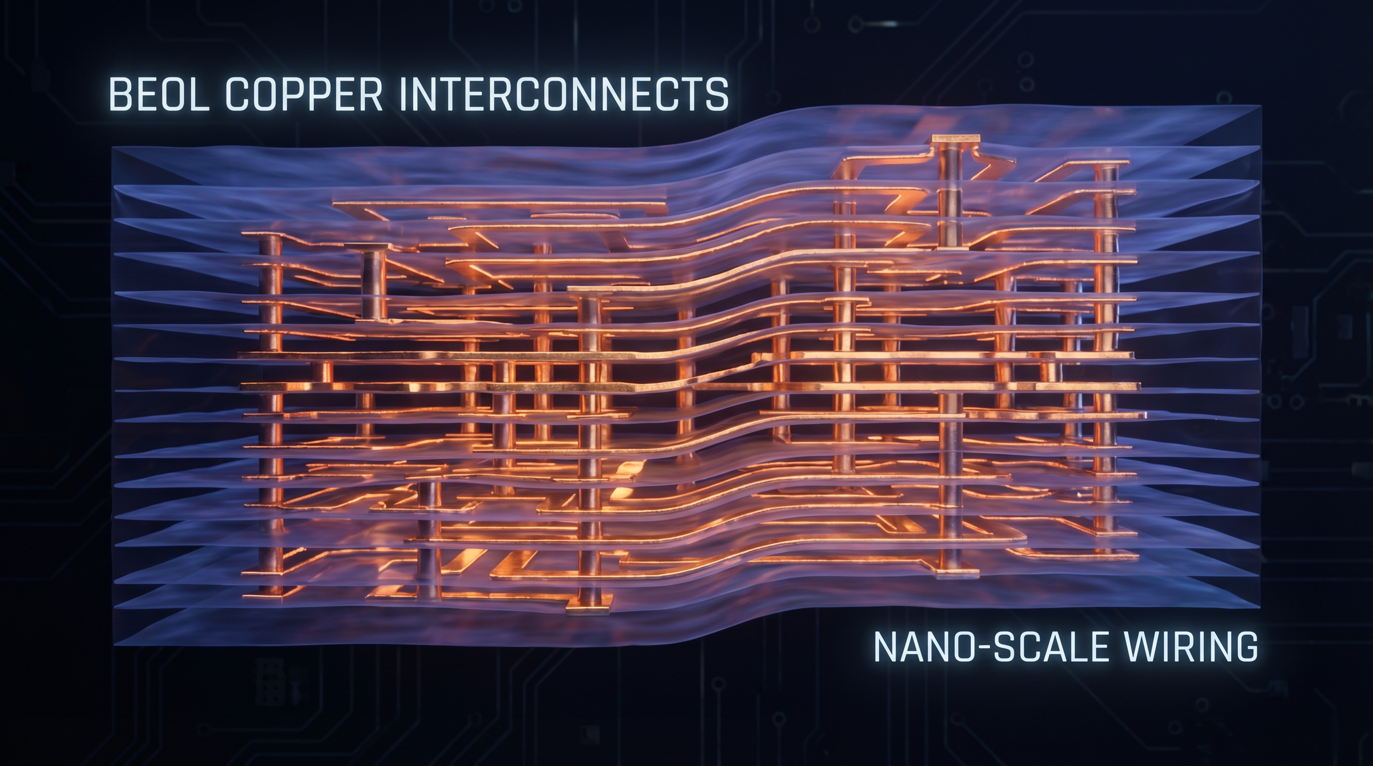
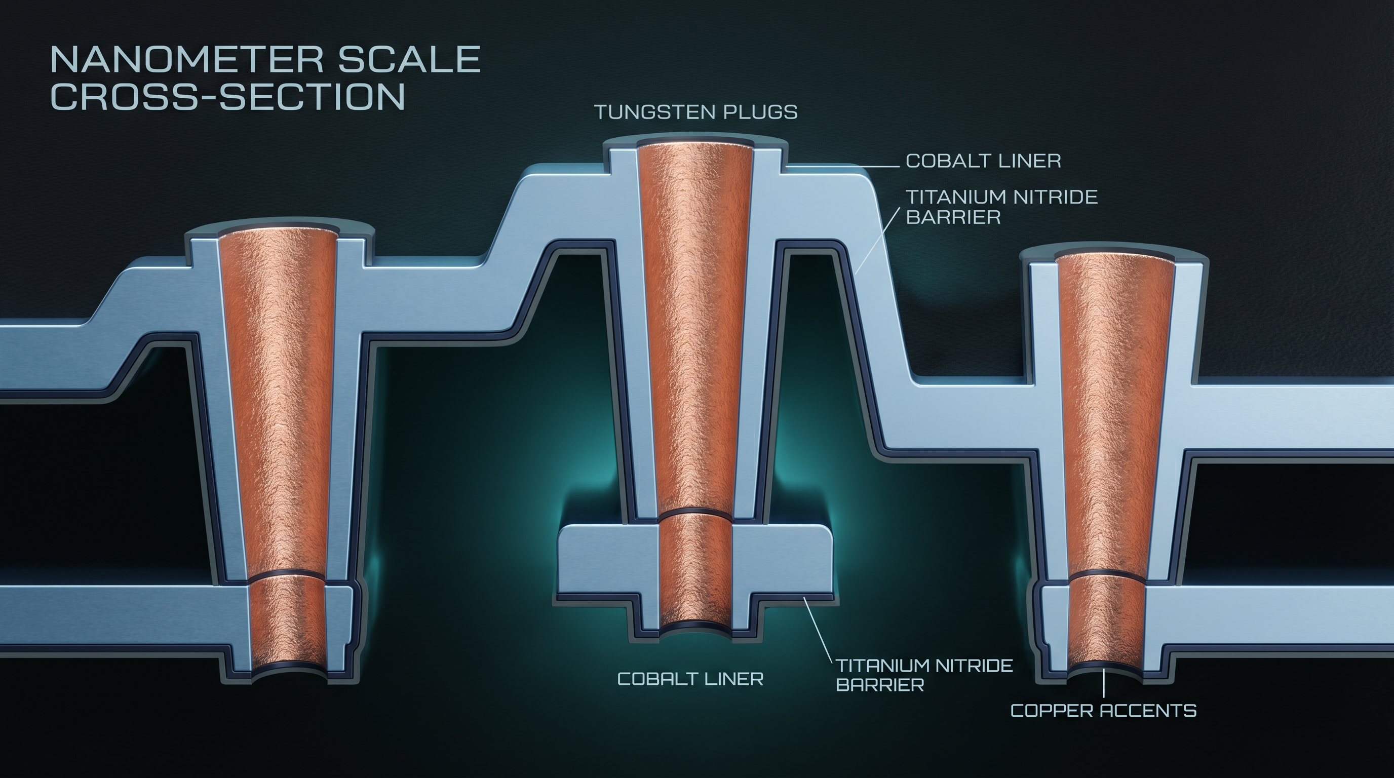
Transistors are useless without wiring. The dual damascene process creates copper interconnects: trenches and vias are etched into low-k dielectric material, then lined with a TaN/Ta barrier layer and copper seed layer (PVD), then filled with electroplated copper. CMP removes the excess copper, leaving buried copper lines. This is repeated 12–20 times, building up a 3D highway system — wide power rails at the top, progressively thinner signal wires toward the transistors. At the M1 (first metal) layer, copper lines are just 12–20nm wide and spaced 20nm apart. The total length of copper wiring in a modern CPU: over 1 kilometer — all compressed into a 10mm × 10mm chip.

Key Stakeholders

Applied Materials Lam Research Tokyo Electron Entegris (chemicals) CMC Materials Atotech (plating chemistry) MacDermid Enthone Cabot Microelectronics

Materials

Copper (electroplating) TaN/Ta barrier Copper seed (PVD) Low-k dielectric Tungsten (vias) CMP slurry

Specifications

Metal layers: 12–20  ·  M1 pitch: 20nm  ·  Copper line width: 12–20nm  ·  Total wire length: ~1 km
STEP 17 Die Scale

Wafer Testing — Wafer Sort

Every die on the wafer is electrically probed and graded

7 companies involved
Wafer probe station — tungsten needle probe card testing every die on a 300mm wafer
Probe Station DIE SCALE Electrical
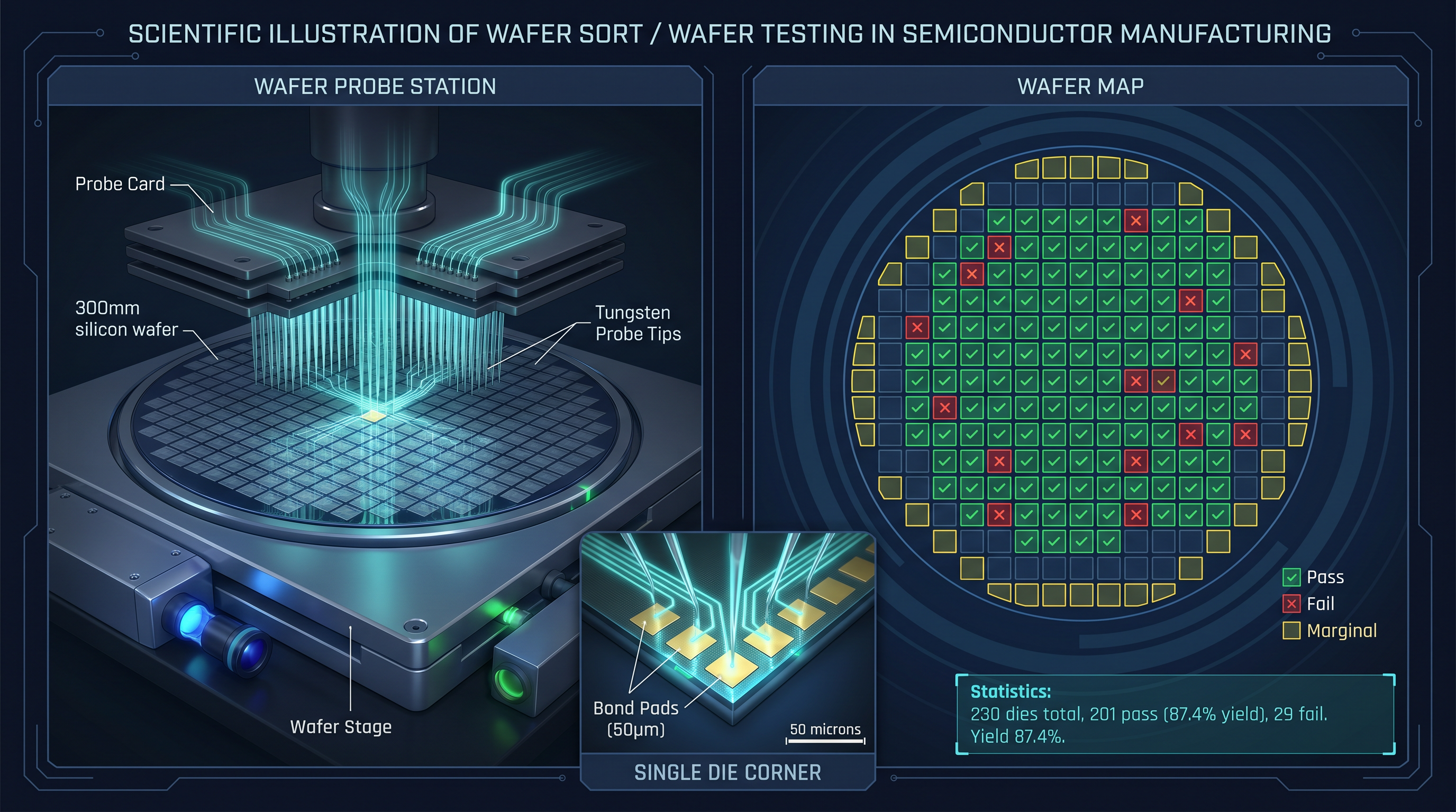
Before the wafer is cut apart, every single die (chip) is tested in place using a probe station. A precision XY stage positions the wafer under a probe card — an array of thousands of tungsten needle tips that contact all the bond pads of one die simultaneously. Automated test equipment (ATE) runs thousands of functional tests: logic tests, memory tests, analog/mixed-signal tests, speed tests, leakage measurements. The test sequence for a complex processor can take 30–90 seconds per die. A map is generated showing which dies pass, fail, or are marginal. Failed dies are inked or mapped for rejection. Wafer sort yield for a new process node starts at 30–50% and improves to 90%+ as the process matures.

Key Stakeholders

Teradyne Advantest KLA Corporation FormFactor (probe cards) Cohu Xcerra Kulicke & Soffa MPI Corporation

Materials

Tungsten probe needles Probe card Thermal chuck (temp-controlled)

Specifications

Test time: 30–90 sec/die  ·  Probe accuracy: ±5μm  ·  Initial yield: 30–50%  ·  Mature yield: 85–95%
THE WAFER AT FULL SCALE

300mm  ·  230 dies per wafer  ·  Each die contains 30 billion transistors

230 Dies per Wafer
300mm Wafer Diameter
0.775mm Thickness
~$100,000 Wafer Value (finished)
30B Transistors / Die
STEP 18 Die Scale → Crystal Scale

Wafer Dicing & Die Separation

Diamond blades or lasers separate hundreds of chips from a single wafer

7 companies involved
Wafer dicing — diamond blade or stealth IR laser separating individual dies from silicon wafer
Dicing Saw DIE SCALE Crystal
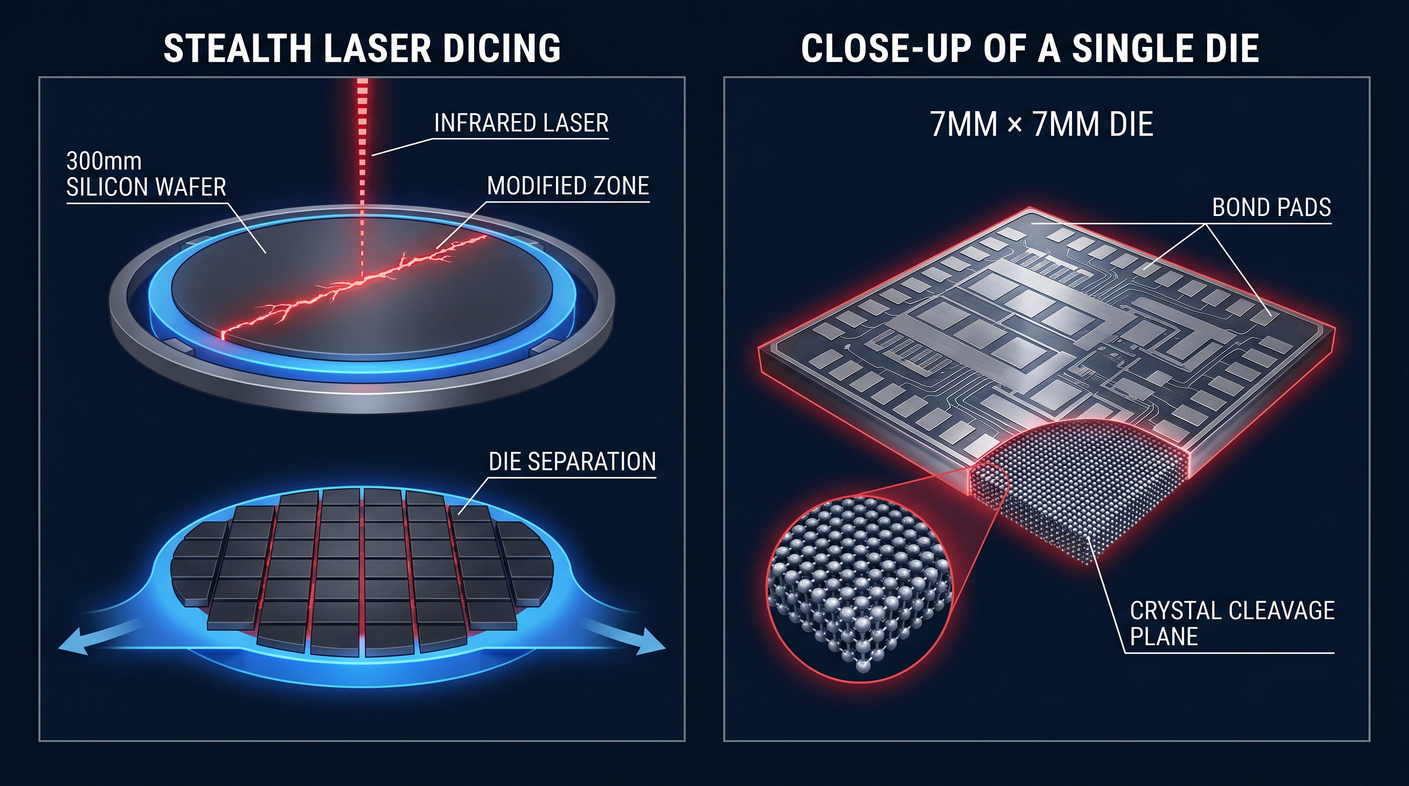
The tested wafer is mounted on blue UV-release dicing tape in a metal ring frame. Two methods are used: Blade dicing uses a diamond-embedded resin blade spinning at 30,000 RPM, cutting through the 0.775mm silicon in a single pass along scribe lines. Stealth dicing uses an infrared laser focused inside the wafer — the modified zone creates a fracture plane, and the tape is then stretched to separate the dies cleanly with zero kerf loss. Laser dicing is preferred for thin wafers and advanced nodes. After dicing, the tape is exposed to UV light (releasing the dies), and robotic pick-and-place systems transfer individual dies to trays for packaging. A 300mm wafer yields 200–500 dies depending on die size.

Key Stakeholders

Disco Corporation Tokyo Seimitsu K&S (Kulicke & Soffa) Synova (laser dicing) Panasonic Factory Solutions ACCRETECH Loadpoint Dynatex International

Materials

Diamond dicing blade UV-release tape DI water cooling IR laser (stealth dicing)

Specifications

Blade speed: 30,000 RPM  ·  Kerf: 30–70μm (blade) / 0μm (stealth)  ·  Die separation accuracy: ±5μm
STEP 19 Chip Scale

Advanced Packaging — OSAT

The bare die is bonded, encased, and connected to the outside world

8 companies involved
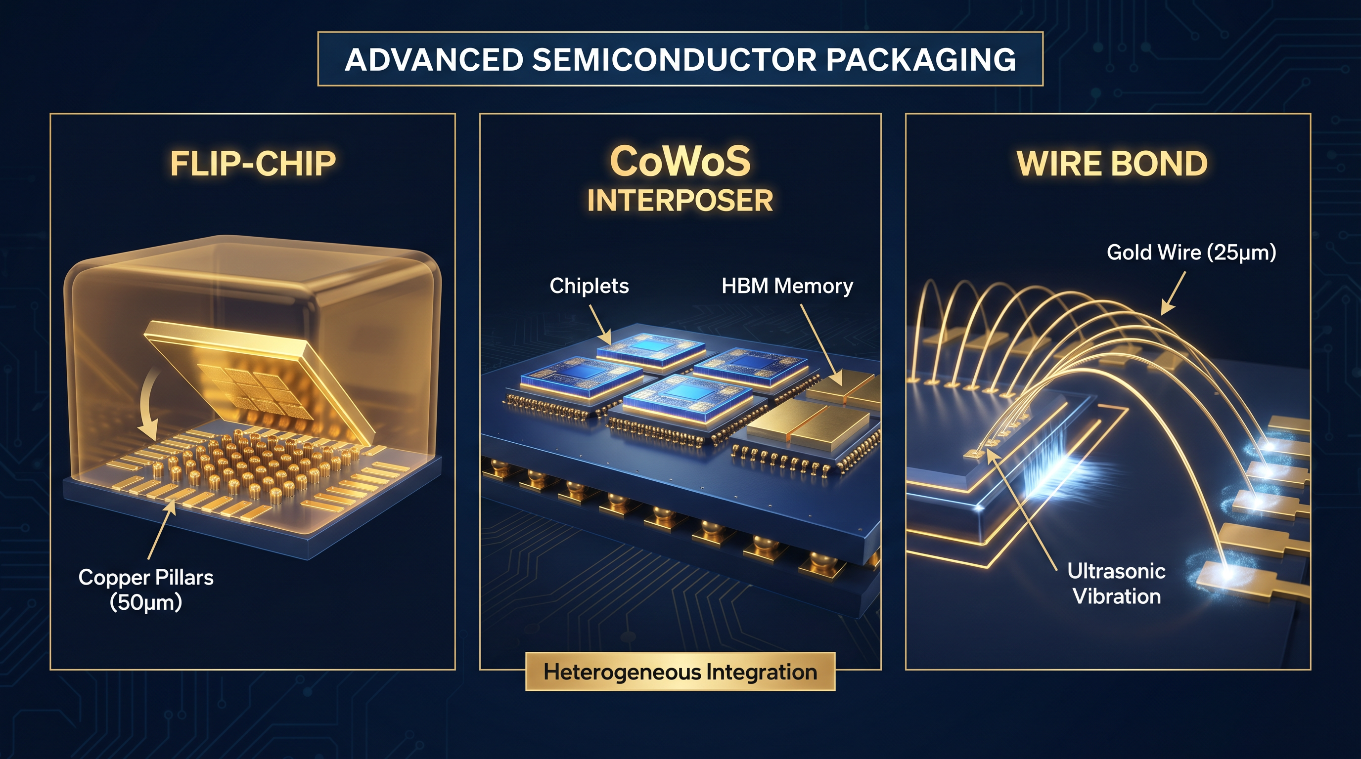
Advanced chip packaging — flip chip bonding, wire bonding, and CoWoS integration
OSAT Facility Bond Pads Cu Pillar
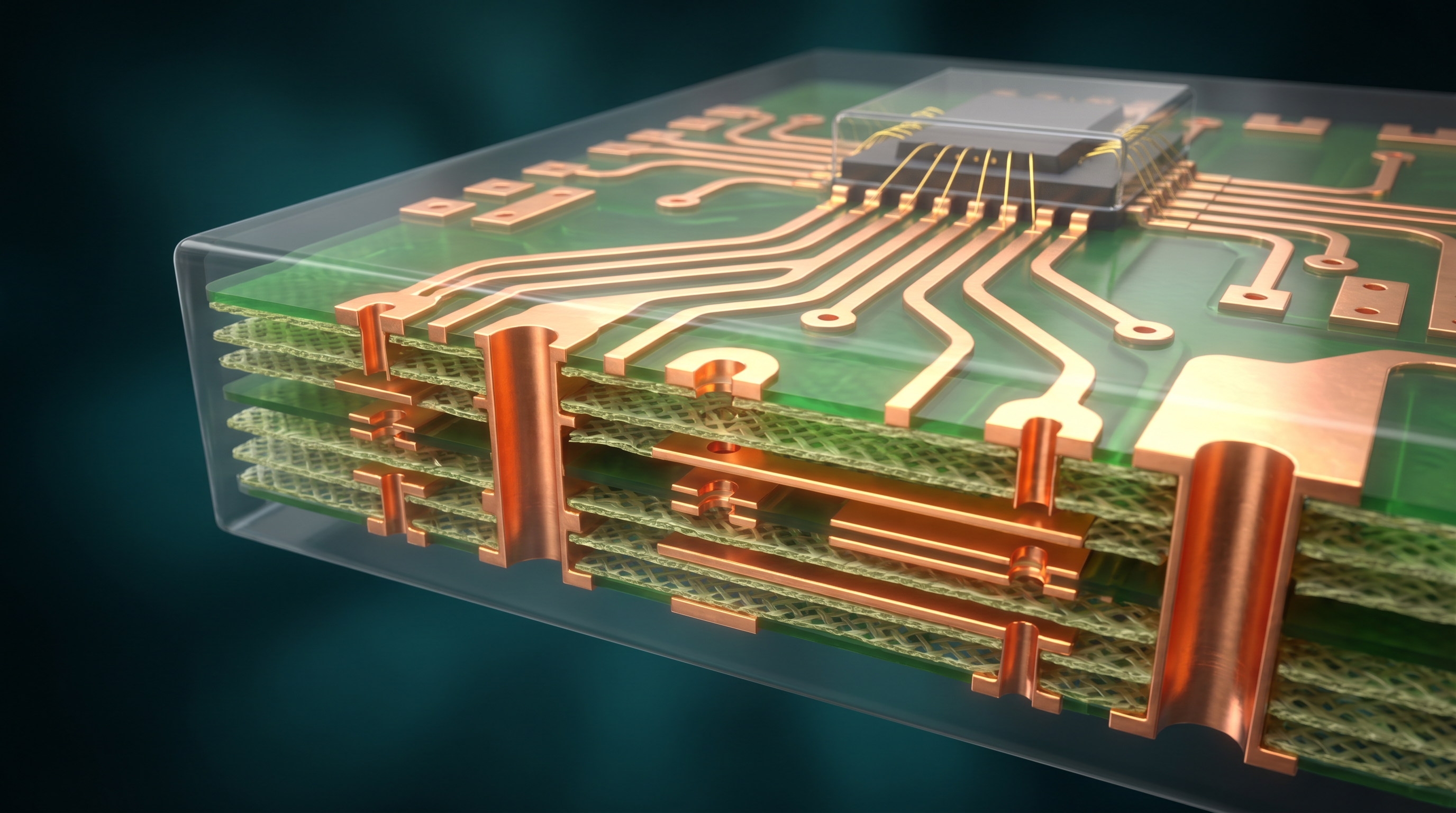
The bare silicon die is fragile, cannot be handled, and has no external connections. Packaging protects it and connects its nanoscale bond pads to PCB-scale pins. Modern packaging includes: Flip-chip — copper pillar bumps (50μm) connect the die face-down to a substrate; Wire bonding — 25μm gold or aluminum wires looped from die pads to package leads by ultrasonic bonding; Advanced packages like CoWoS (Chip on Wafer on Substrate) stack multiple chiplets and HBM memory on a silicon interposer for AI chips. The package is then encapsulated in epoxy mold compound for protection. OSAT (Outsourced Semiconductor Assembly and Test) companies like ASE and Amkor perform this step for most chipmakers.

Key Stakeholders

ASE Group Amkor Technology JCET (STATS ChipPAC) Powertech Technology SPIL TSMC Advanced Packaging (CoWoS) Samsung Intel (EMIB) Henkel (epoxy)

Materials

Copper pillar bumps Gold wire (25μm) Epoxy mold compound Substrate (BGA/LGA) Underfill epoxy

Specifications

Copper pillar: 50μm diameter  ·  Gold wire: 25μm  ·  CoWoS bump pitch: 55μm  ·  Mold temp: 175°C
STEP 20 System Scale

Final Testing, Burn-In & Global Shipment

Every chip runs at full stress for hours before it leaves the factory

8 companies involved
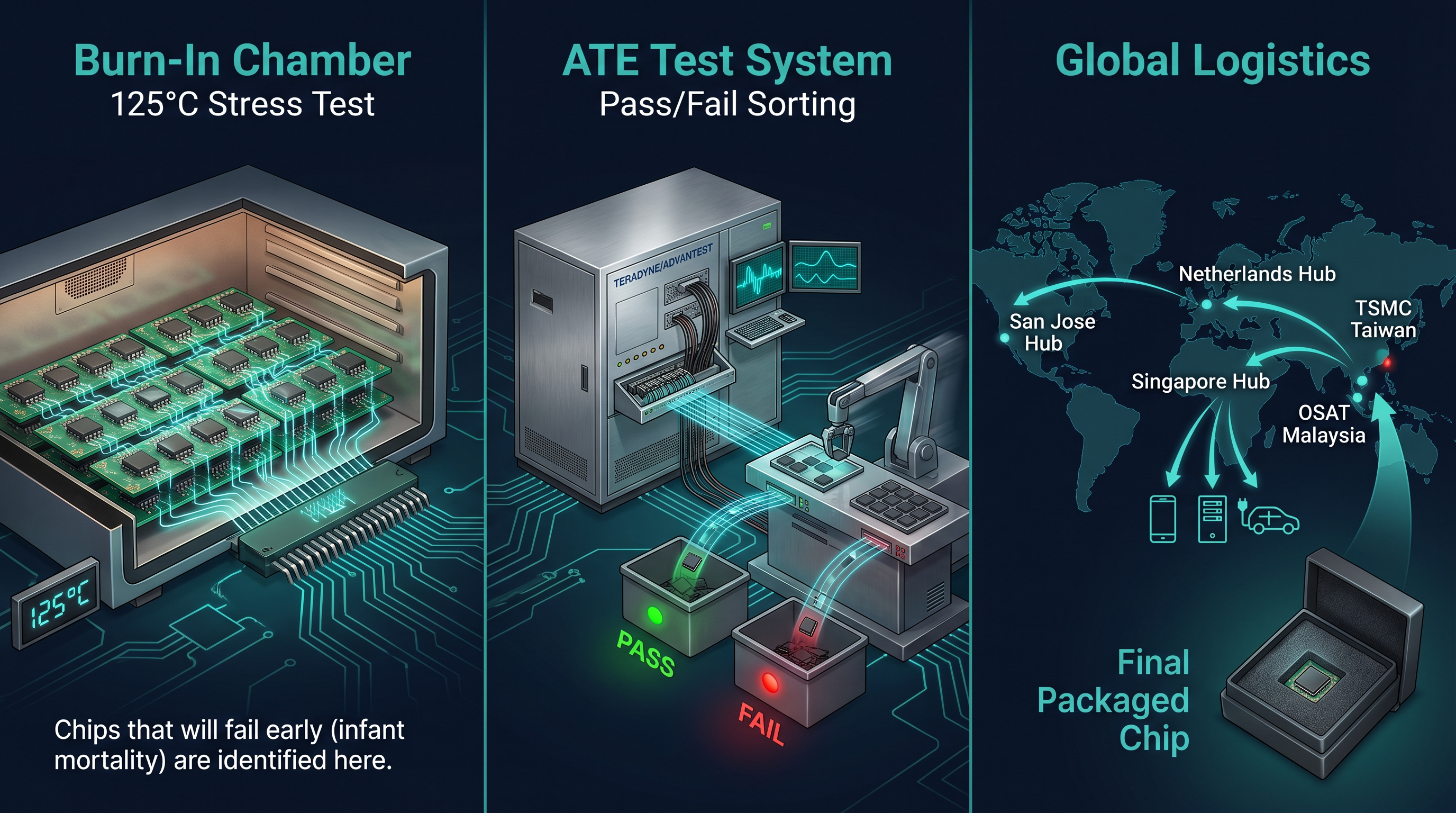
Final chip testing and burn-in — packaged chips undergoing stress testing at 125°C
Test Floor Package System
Packaged chips undergo final system-level testing to catch any packaging-induced failures. Burn-in stress testing runs chips at elevated temperature (125°C) and voltage for 24–168 hours — this accelerated stress screens out "infant mortality" failures (devices that would fail early in use due to marginal defects). Automated test equipment runs full parametric, functional, and speed-grade testing. Chips are sorted by performance: the fastest become premium-tier parts, medium speed becomes mainstream, and slow parts become budget or embedded chips. This "binning" maximizes yield value. Chips are then packed in moisture-barrier bags, placed in trays or tape-and-reel, and air-freighted globally. The average semiconductor chip travels through 25+ countries across its supply chain before reaching a consumer device.

Key Stakeholders

Teradyne Advantest Cohu UTAC Group UMC (back-end) Amkor Intel (ISP) Qualcomm (fabless) Apple (fabless)

Materials

Test sockets Burn-in boards Moisture barrier bags Desiccant Tape-and-reel packaging

Specifications

Burn-in: 125°C  ·  Duration: 24–168 hours  ·  Supply chain: 25+ countries  ·  Lead time: 3–6 months
THE CHEMISTRY OF CHIP MAKING

Semiconductor manufacturing consumes hundreds of specialty gases and chemicals. Here are the most critical.

SiH₄ Silane Step 9: CVD Silicon source gas for CVD deposition of polysilicon and silicon nitride films
NH₃ Ammonia Step 9: Nitride Nitrogen source for Si₃N₄ (silicon nitride) deposition via CVD/ALD
HF Hydrogen Fluoride Step 12: Etch Selective oxide removal in wet etching. Also used in wafer cleaning (dilute HF)
Cl₂ Chlorine Step 12: Dry Etch Poly-silicon and metal (Al, W, TiN) dry etching in RIE plasma
Ar Argon Steps 4, 9, 13 Carrier gas, PVD sputtering medium, and ion implant beam transport
N₂ Nitrogen All Steps Purge gas, blanket atmosphere for oxidation-sensitive steps, carrier gas
O₂ Oxygen Step 8: Oxidation Thermal oxide (SiO₂) growth for gate dielectric and isolation layers
H₂ Hydrogen Step 3: Epi Carrier gas for epitaxial silicon growth; also used in wet oxidation (steam)
NF₃ Nitrogen Trifluoride All: Chamber Clean Remote plasma chamber cleaning — removes silicon and silicon nitride buildup from CVD chambers
WF₆ Tungsten Hexafluoride Step 16: Metal CVD tungsten deposition for contact and via fill in back-end-of-line metallization